What Are the Reasons for BGA Soldering Defects?
By:PCBBUY 09/25/2024 15:55
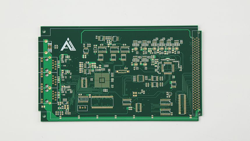
Ball Grid Array (BGA) soldering is a critical process in modern electronics assembly. This technique is widely used due to its advantages in space efficiency and performance. However, like any manufacturing process, it is susceptible to defects that can compromise the reliability of the finished product. This article explores the various reasons behind BGA soldering defects, supported by scientific principles, data, and comparisons.
1. Introduction
BGA soldering defects can lead to failures in electronic devices, making it essential to understand the root causes. This article aims to provide an in-depth analysis of the reasons for these defects, emphasizing the interplay of materials, processes, and environmental conditions.

2. Overview of BGA Technology
BGA is a type of surface-mount packaging used for integrated circuits. It consists of an array of solder balls on the bottom of the package, which are melted during soldering to create electrical connections. This technology offers several advantages, including:
Reduced Footprint: BGA packages take up less space compared to traditional leaded packages.
Improved Electrical Performance: The short distance between the chip and PCB reduces inductance and improves performance.
Enhanced Thermal Management: The larger solder balls allow for better heat dissipation.
3. Principles of BGA Soldering
The BGA soldering process involves several steps, including placement, reflow, and cooling. During reflow, the solder balls melt and form a bond with the PCB pads. The key principles include:
1. Thermal Transfer: Heat is applied uniformly to melt the solder.
2. Surface Tension: Once melted, the solder's surface tension aids in wetting the pad.
3. Capillary Action: This phenomenon helps in pulling the molten solder into the joint.
The general reaction for the solder melting can be represented as:
Sn+Ag→SnxAgy
Where Sn is tin and Ag is silver, typical components of solder alloys.

4. Common BGA Soldering Defects
4.1 Insufficient Wetting
Definition: Insufficient wetting occurs when the solder does not adequately flow onto the PCB pad.
Causes:
Contaminated surfaces (e.g., oils, oxidation).
Incorrect solder paste viscosity.
4.2 Solder Balling
Definition: Solder balling refers to the formation of small, unwanted solder balls on the PCB surface.
Causes:
Excessive solder paste application.
Inconsistent thermal profiles during reflow.
4.3 Cold Solder Joints
Definition: Cold solder joints are weak connections formed when solder does not fully melt or bond.
Causes:
Inadequate heating during reflow.
Movement of the component during the cooling phase.
4.4 Bridging
Definition: Bridging occurs when solder connects two adjacent pads, causing electrical shorts.
Causes:
Too much solder paste applied.
Improper stencil design.
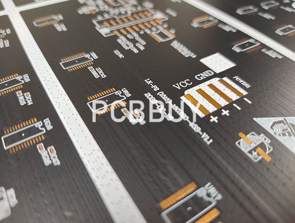
4.5 Tombstoning
Definition: Tombstoning is a defect where one side of a component lifts off the PCB, resembling a tombstone.
Causes:
Uneven heating during the reflow process.
Asymmetrical solder paste deposition.
5. Factors Contributing to BGA Soldering Defects
5.1 Material Issues
Solder Alloy Composition: The composition of the solder alloy can affect its performance. Common alloys include SAC305 (96.5% Sn, 3% Ag, 0.5% Cu) and SAC405 (95.5% Sn, 4% Ag, 0.5% Cu).
|
Solder Alloy |
Melting Point (°C) |
Tensile Strength (MPa) |
|
SAC305 |
217 |
55-70 |
|
SAC405 |
217 |
55-70 |
5.2 Process Parameters
Reflow Temperature Profile: A proper thermal profile is crucial. The typical reflow temperature for SAC alloys is between 217°C and 260°C.
Preheat Zone: 150°C - 180°C
Soak Zone: 180°C - 210°C
Reflow Zone: 217°C - 260°C
5.3 Environmental Factors
Humidity: High humidity can lead to oxidation of the solder balls, affecting wetting.
Contamination: Dust and particles on the PCB can inhibit solder flow.
5.4 Design Considerations
Pad Design: The size and shape of pads significantly influence solder joint quality. A common design rule is to have pads that are at least 1.5 times the size of the solder balls.
Component Placement: Proper alignment and placement are crucial for effective soldering.

6. Mitigation Strategies
1. Surface Preparation: Ensure PCB pads are clean and free of contaminants.
2. Optimized Solder Paste Application: Use appropriate stencil designs and techniques to control solder paste deposition.
3. Controlled Reflow Profiles: Regularly monitor and adjust reflow oven settings to ensure consistent heating.
4. Regular Equipment Maintenance: Maintain soldering equipment to prevent mechanical failures.
5. Training: Provide thorough training for operators on the BGA soldering process and best practices.
Conclusion
BGA soldering defects can arise from a variety of factors, including material selection, process parameters, environmental conditions, and design considerations. Understanding these reasons is crucial for improving the reliability of electronic assemblies. By implementing effective mitigation strategies, manufacturers can significantly reduce the occurrence of these defects and enhance product quality.
References
1. R. C. Lee and C. W. M. Chang, BGA Reliability: A Review," Journal of Electronic Materials, vol. 44, no. 3, pp. 762-775, 2015.
2. D. A. G. Lima et al., Thermal and Mechanical Analysis of BGA Solder Joints, Microelectronics Reliability*, vol. 81, pp. 1-10, 2018.
3. A. Y. Chien, The Science and Technology of Soldering," Soldering & Surface Mount Technology, vol. 19, no. 1, pp. 30-35, 2007.
4. IPC-7095, "Design and Assembly Process for BGAs," IPC, 2018.
5. S. R. Norrgard, "Common BGA Assembly Defects and Their Solutions," Electronics Manufacturing Magazine, vol. 25, no. 4, pp. 22-29, 2019.
Industry Category


