What Are the Rules PCB Ground Plane?
By:PCBBUY 02/22/2024 16:05

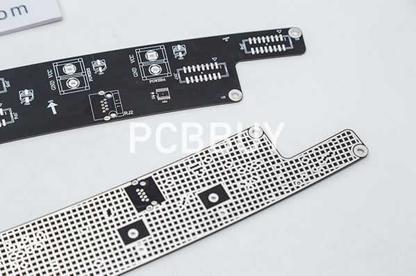
One common technique is to use a ground plane, which is a large piece of copper on a PCB. Typically, PCB manufacturers will cover all of the areas that don’t have a component or trace on them with the copper ground plane. In a two-layer board, the standard PCB ground plane rules indicate that the ground plane should be placed on the board’s bottom layer, while the components and signal traces are on the top layer.
Do you know the methods about ground plane PCB? If you are curious about the professional knowledge about ground plane PCB, please check and read the content in this passage.
What is PCB plane capacitor?
This is not a major benefit, and it applies only to ground planes that are adjacent to a power plane. I think it’s still worth mentioning, though. A ground plane separated from a power plane by a thin dielectric sounds a lot like a parallel-plate capacitor, and that’s exactly what it is. This structure adds a bit of distributed power-supply capacitance to your entire circuit board, though it certainly isn’t going to replace your decoupling capacitors.
A solid ground plane provides some degree of protection against electromagnetic interference (both radiated and received). I wouldn’t rely on a ground plane to solve all of your EMI problems, especially if you have components on both sides of the board; a carefully designed conductive enclosure would be more effective. Nonetheless, every little bit helps, and if you’re concerned about EMI then you have one more reason to incorporate a ground plane into your layout.

Why Is the PCB Ground Plane Important?
The ground plane on a printed circuit board is typically a large area of metal connected to the circuit ground. This area of metal is sometimes only a small portion of the board, or in a multi-layer design it may be one entire board layer. Depending on the needs of the design, it may even occupy multiple layers.
The ground plane serves three important purposes in a printed circuit board:
Voltage return: Most every component on the PCB will connect to a power net, and then the return voltage will come back through the ground net. On boards with only one or two layers, ground nets usually have to be routed using wider traces. By devoting an entire layer to the ground plane in a multi-layer board however, it simplifies connecting each component to the ground net.
Signal return: Regular signals also need to return, and with high speed designs it is very important that they have a clear return path on the ground plane. Without this clear return path these signals can generate a lot of interference for the rest of the PCB.
Reduce noise and interference: As signal speeds increase, there are more digital circuits switching states. This creates noise pulses through the ground circuit that may affect other parts of the circuit. A ground plane with its large conducting area helps reduce the amount of this disturbance because it has lower impedance than if the ground net is routed through a trace.

What Are the Rules PCB Ground Plane?
Maybe you’ve designed a digital device with some variance in your ground and data can still move safely around. However, consider something like a high-reliability medical system. If that device gets zapped with a high-voltage ESD charge, you better hope you properly designed your ground. In sensitive electronic designs such as these, proper grounding can mean the difference between life and death.
Leave nothing unattached
Nothing should remain unattached on your PCB layout. If there’s an open space on your board, fill it with copper and vias to connect with your ground plane. This will create a structured path for all of your signals to efficiently get to ground.
Never slice up your ground layer
Most engineers working on four layer boards will have a dedicated ground layer. This works great as long as you don’t route traces on this layer. Once you do, you’ve effectively created a ground current loop. Keep your ground layer whole at all times.

Grounding before routing
A poorly designed ground puts your entire device at risk. The same can’t be said for messing up a single signal. Be sure to properly design your ground first before doing any routing. This will serve as the foundation for your entire routing process.
Know where your currents are going
Many designers only think about where their signal is traveling to, but every signal has a return path to take through ground. Both the sending and return path of your signal will have the same current which can affect power stability and ground bounce. You can use Kirchhoff’s Current Law to understand how current will travel through your circuit.
Industry Category


