What Are the Specialty PCBs?
By:PCBBUY 04/25/2025 14:59
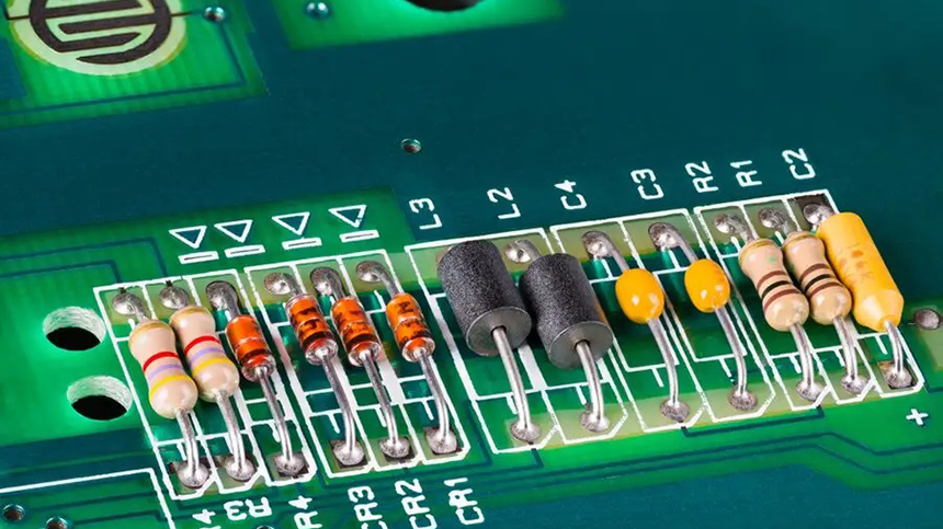
Printed Circuit Boards (PCBs) are the backbone of electronic devices, facilitating electrical connections and mechanical support for various components. While traditional PCBs are ubiquitous in consumer electronics, specialized PCBs are crucial in applications requiring unique performance characteristics. This article delves into three such specialty PCBs: High-Frequency PCBs, Metal Core PCBs, and Thick Copper PCBs, discussing their characteristics, structure, manufacturing processes, and associated challenges.
High-Frequency PCBs
Characteristics and Applications
High-Frequency: PCBs are designed to handle signals in the gigahertz (GHz) range. They are essential in applications such as:
Telecommunications: Wireless networks and satellite communications.
Aerospace and Defense: Radar and missile guidance systems.
Medical Devices: Imaging equipment like MRI and CT scanners.
Automotive Electronics: Advanced driver-assistance systems (ADAS).
Structure and Materials
The performance of high-frequency: PCBs is heavily dependent on the materials used. Common materials include:
Rogers Laminates: Known for their low dielectric constant and low loss tangent, essential for high-frequency signal integrity.
Teflon (PTFE): Offers excellent electrical properties but is challenging to process.
Ceramics: Provide high thermal stability and low electrical loss.
The typical structure involves multiple layers, including signal layers, ground planes, and power planes, designed to minimize signal loss and crosstalk. The materials used must have:
Low Dielectric Constant (Dk): To reduce signal delay.
Low Dissipation Factor (Df): To minimize signal loss.
Thermal Stability: To maintain performance under varying temperatures.
Manufacturing Processes and Challenges
Multilayer PCB Fabrication
High-frequency PCBs often require multilayer configurations to accommodate complex circuitry and shielding requirements. The fabrication process includes:
1. Lamination: Using materials like Rogers or Teflon, layers are bonded under heat and pressure.
2. Drilling: Precision drilling techniques, often with laser drills, are used to create vias.
3. Plating: Vias are plated with copper to ensure electrical connectivity.
4. Etching: Advanced photolithography is used to define intricate circuit patterns.
5. Testing: High-frequency testing to ensure signal integrity and impedance control.

Process Challenges
Material Handling: Teflon and ceramic materials can be difficult to laminate and process due to their physical properties.
Impedance Control: Maintaining tight impedance tolerances is critical for signal integrity, requiring precise manufacturing controls.
Thermal Management: High-frequency operation generates significant heat, necessitating effective thermal management solutions.
Data Table: Material Properties Comparison
|
Material |
Dielectric Constant (Dk |
Dissipation Factor (Df) |
Thermal Conductivity (W/m·K) |
|
Rogers 4350 |
3.48 |
0.0037 |
0.64 |
|
PTFE |
2.1 |
0.0002 |
0.25 |
|
Ceramics |
4.5 |
0.001 |
20 |
Metal Core PCBs
Characteristics and Applications
Metal Core PCBs (MCPCBs) are designed to enhance thermal management, making them suitable for applications such as:
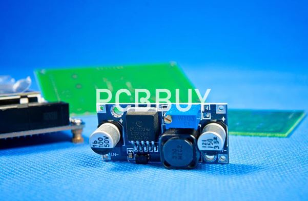
LED Lighting: High-power LEDs require efficient heat dissipation.
Power Electronics: Inverters and power supplies.
Automotive: Engine control units and power modules.
Industrial Equipment: Motor drives and high-power devices.
Structure and Materials
MCPCBs typically consist of three layers:
1. Metal Core: Usually aluminum or copper, providing excellent thermal conductivity.
2. Dielectric Layer: An insulating layer with high thermal conductivity.
3. Copper Circuit Layer: Where the electronic components are mounted.
The metal core acts as a heat sink, efficiently dissipating heat away from the components. The dielectric layer ensures electrical insulation while allowing heat transfer.
Manufacturing Processes and Challenges
Multilayer PCB Fabrication
1. Lamination: Layers are laminated with a metal core, using high thermal conductivity prepregs.
2. Drilling: Mechanical drilling is used to create vias and mounting holes.
3. Plating: Copper plating for vias and surface finishes.
4. Etching: Patterning the copper circuit layer using photolithography.
5. Solder Mask and Surface Finish: Applying protective solder mask and surface finishes like HASL or ENIG.
Process Challenges
Thermal Management: Ensuring efficient heat transfer from the components to the metal core.
Material Selection: Balancing thermal conductivity and electrical insulation in the dielectric layer.
Mechanical Stability: Managing stresses due to different coefficients of thermal expansion (CTE) between layers.
Data Table: Metal Core Material Properties
|
Property |
Aluminum Core |
Copper Core |
|
Thermal Conductivity (W/m·K) |
200 |
400 |
|
Electrical Conductivity |
Good |
Excellent |
|
Density (g/cm³) |
2.7 |
8.96 |
Thick Copper PCBs
Characteristics and Applications
Thick Copper PCBs are used in high-current and high-power applications due to their ability to handle large currents without excessive heating. Applications include:
Power Supply Systems: High-current power supplies.
Automotive: Electric vehicle power electronics.
Industrial Equipment: Heavy machinery control systems.
Renewable Energy: Solar panel inverters and wind turbine converters.
Structure and Materials
Thick Copper: PCBs can feature copper thicknesses ranging from 2oz/ft² to 10oz/ft² or more. They typically consist of:
Copper Layers: Thick copper layers to handle high currents.
Prepreg and Laminate: Standard FR-4 or high-performance laminates.
Multiple Layers: To distribute high current and manage heat.
Manufacturing Processes and Challenges
Multilayer PCB Fabrication
1. Copper Plating: Applying thick copper layers through electroplating.
2. Etching: Using stronger etching solutions to define circuit patterns in thick copper.
3. Lamination: Laminating multiple layers with thick copper.
4. Drilling and Plating: Creating and plating vias to handle high currents.
5. Solder Mask and Surface Finish: Applying protective layers and surface finishes.
Process Challenges
Etching: Achieving precise patterns with thick copper is challenging due to the depth of etching required.
Thermal Management: Thick copper layers can cause differential heating, requiring careful thermal management.
Mechanical Stability: Ensuring structural integrity with thick copper layers.
Data Table: Copper Thickness and Current Capacity
|
Copper Thickness (oz/ft²) |
Current Capacity (A) |
Recommended Trace Width (mm) |
|
2 |
30 |
1.5 |
|
4 |
60 |
2.5 |
|
6 |
90 |
3.5 |
|
10 |
150 |
5.0 |
Specialty PCBs such as High-Frequency PCBs, Metal Core PCBs, and Thick Copper PCBs play crucial roles in various advanced applications, each addressing specific requirements through their unique structures and materials. Understanding their characteristics, manufacturing processes, and challenges is essential for optimizing their performance in demanding environments.
References
1.Rogers Corporation. (2020). High-Frequency Laminates. Retrieved from [rogerscorp.com] (https://www.rogerscorp.com)
2.Isola Group. (2019). Metal Core PCB Materials. Retrieved from [isola-group.com] (https://www.isola-group.com)
3. IPC Standards. (2021). Design and Manufacturing Standards for Thick Copper PCBs. Retrieved from [ipc.org] (https://www.ipc.org)
Industry Category


