What Are the Status, Classification, and Characteristics of Special PCB?
By:PCBBUY 07/05/2024 17:29
Overview
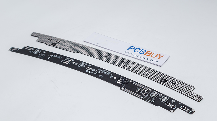
In 2006, the Electronic Information Products Management Division of the Ministry of Information Industry (now the Ministry of Industry and Information Technology) summarized high-end PCB product types as HDI boards, multi-layer FPCs, rigid-flex boards, IC substrates, communication backplanes, special material PCBs, and new types of PCBs. However, there is still no complete definition of special printed circuit boards in the field of PCB design and manufacturing. The general consensus is that special printed circuit boards refer to those with unique manufacturing materials, special product applications, and distinctive manufacturing processes.
![]()
The specialization of materials for special printed circuit boards is determined by their functions and performance requirements in electronic equipment. The substrate material acts as a carrier for PCB traces and components. With the increasing frequency and speed of electronic signal transmission and the rise in layer counts, low electromagnetic interference, high signal integrity, and high heat dissipation have become essential qualities for new products. These performance requirements can no longer be met by circuit design alone, making the selection of new materials a key direction for technological progress. For high-frequency signal transmission and high-current transmission applications, low dielectric constant, low loss, and high thermal conductivity materials are used as substrate materials for special printed circuit boards. The choice of these unique substrate materials determines the specialized manufacturing processes.
With the widespread use of electronic products in daily life, industrial production, and scientific innovation, special printed circuit boards are increasingly being used in fields such as communication electronics, consumer electronics, automotive electronics, instruments, and power supplies. According to statistics from WECC (World Electronic Circuit Council), IPC (Association Connecting Electronics Industries), and CPCA (China Printed Circuit Association):
1. In 2007, the global PCB output value was $50.9 billion, with special boards accounting for $2.3 billion, or 4.5% of the total.
2. In 2014, China's PCB output value was 170 billion RMB, with special boards accounting for about 10.2 billion RMB, or 6.0% of the total.
What Is Metal Core PCB Manufacturing Technology?
As electronic products develop towards being lighter, thinner, smaller, higher in density, and more multifunctional, the design linewidth of printed circuit boards becomes finer, the copper area smaller, the spacing between components closer, and the assembly density and integration higher. Power consumption increases, making thermal management solutions increasingly important, and the need for improved thermal conductivity of PCB substrates more urgent. Poor thermal conductivity of the substrate leads to slower heat dissipation, causing components on the PCB to overheat, which can result in component aging, failure, shortened lifespan, and reduced reliability of the entire system. One solution to this problem is the use of metal core printed circuit boards.
What Is Overview of Metal Core PCB?
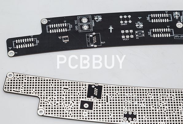
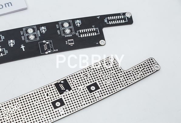
Metal core printed circuit boards (MCPCBs) consist of a metal substrate with excellent thermal conductivity, an insulating dielectric layer, and a copper trace layer, forming a high-thermal-conductivity PCB with a sandwich structure as shown in Figure 3-1. The demand for high-frequency communication signals, high-definition, and large data transfer has driven continuous innovation in PCB manufacturing technology. High-frequency and high-speed signal transmission requires strict material standards, ensuring not only the creation of metal traces on an insulating substrate for connectivity but also the quality of signal transmission. In fields such as microwave applications and high-power electronics (e.g., LED applications), the thermal properties of materials significantly impact system reliability. In high-reliability, high-power, high-frequency applications such as military radars, microwave applications, missile control systems, and GPS power amplifiers, conventional thermal management methods are inadequate, making materials with good thermal conductivity a necessity. Practical applications have shown that using metal substrates for thermal solutions, as opposed to traditional heat sinks and fans, can greatly reduce equipment size and manufacturing costs.
For MCPCBs with a three-layer sandwich structure, the material selection and manufacturing processes for each layer are unique. The metal substrate layer can theoretically be any metal with good thermal conductivity, but due to cost and manufacturability constraints, common materials include aluminum, iron, copper, invar, and tungsten-molybdenum alloys. This layer provides physical support and a thermal pathway for the circuits and components. Among these, aluminum is favored for its abundant resources, mature manufacturing processes, relatively low cost, good thermal conductivity, ease of processing, and environmental friendliness. Aluminum-based PCBs offer advantages such as economical material costs, reliable electronic connections, high thermal and mechanical strength, and lead-free soldering, making them a key focus of research and application.
The insulating dielectric layer typically uses modified epoxy resins, polyphenylene ether (PPE), or polyimide (PI). Its primary function is to prevent short circuits between the trace layer and the metal substrate. The trace layer, created by etching copper foil, is the main unit for electrical signal and current transmission on the PCB. High thermal conductivity MCPCBs have developed various types, including planar thick copper-based PCBs, aluminum-based PCBs, aluminum core double-sided PCBs, planar copper-based PCBs, aluminum cavity PCBs, metal block-embedded PCBs, and flexible aluminum-based PCBs, which are widely used in consumer electronics, automotive, military, aerospace, and other fields. The key to their performance lies in the adhesive properties between the metal substrate and the circuit layer.
What Are Material Properties and Structure of Metal Core PCB?
Material Characteristics of Metal Core PCBs
It is well known that the thermal conductivity of metal materials is significantly higher than that of synthetic resin materials (and the dielectric they form). This is the theoretical basis for using metal materials as PCB substrates to address the performance degradation of high-heat electronic components. However, metal materials have the disadvantage of high density, making metal core PCBs heavier than organic-based PCBs of the same specifications.
What Are Types, Structures, and Performance of Metal Core PCBs?
Types of Metal Core Copper Clad Laminates
Metal core copper clad laminates (MCCLs) are the base materials for manufacturing metal core PCBs. Their structure and manufacturing methods are similar to those of conventional organic resin-based copper clad laminates (CCLs). MCCLs generally consist of three layers: a copper foil layer, an insulating layer, and a metal layer (such as copper, aluminum, iron, steel, invar, tungsten-molybdenum alloy).
Based on the type of metal used, MCCLs can be classified into aluminum-based CCLs, copper-based CCLs, iron-based CCLs, and tungsten-molybdenum alloy CCLs, with aluminum-based, copper-based, and iron-based CCLs being the most widely used.
1. Aluminum-Based Substrates: Commonly used aluminum materials include LF, LAM, and LY12, meeting the national aluminum alloy manufacturing standards GB/T3880-2006. Performance requirements include tensile strength of 294 N/mm², elongation of 5%, and thermal conductivity of 150-210 W/(m·K). Common thicknesses are 1.0 mm, 1.6 mm, 2.0 mm, and 3.2 mm.
2. Copper-Based Substrates: Typically use red copper sheets, meeting national standards GB/T26017-2010, with performance requirements including tensile strength of 245-217 N/mm², elongation of 15%, and thermal conductivity of 403 W/(m·K). Common thicknesses are 1.0 mm, 1.6 mm, 2.0 mm, 2.36 mm, and 3.2 mm.
3. Iron-Based Substrates: Generally use cold-rolled steel plates or low-carbon steel plates, with performance requirements of 25-32 kg·F/mm² tensile strength and 15% elongation. Common thicknesses include non-phosphorous 1.0 mm and 2.3 mm types, and phosphorous iron bases with 0.5 mm, 0.8 mm, and 1.0 mm thicknesses.
Performance Comparison of Common Metal Substrates
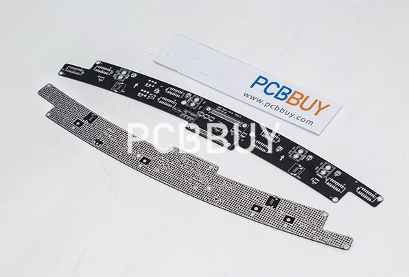
The three main types of metal substrates used in industrial manufacturing are copper, iron, and aluminum substrates, with their performance compared as follows:
1. Copper Substrates: Excellent thermal conductivity, used for heat conduction and electromagnetic shielding, but heavy and expensive.
2. Iron Substrates: Best for electromagnetic interference shielding but with slightly poorer thermal conductivity and cheaper.
3. Aluminum Substrates: Good thermal conductivity, lightweight, decent electromagnetic shielding, but poor resistance to salt corrosion.
Aluminum-based CCLs are currently the most widely used metal substrates due to their superior electrical performance, thermal conductivity, electromagnetic shielding, high voltage resistance, and bendability. Aluminum-based PCBs are extensively used in high-power LED lighting, power supplies, TV backlights, automotive, computers, air conditioner inverters, avionics, medical equipment, audio, and even as essential components in commonly used smartphone cameras.
Functions and Performance of Insulating Layers, Metal Layers, and Conductor Layers in Metal Core PCBs
1. Insulating Layer Performance
The insulating layer in metal core PCBs uses organic polymers (e.g., PET, modified PPE, modified epoxy resins, PI), metal oxides (e.g., Al₂O₃), or ceramics. Its function is to isolate electrical signals between the traces and bond the copper foil layer to the metal layer, providing insulation and adhesion.
The typical thickness of the insulating layer in metal core PCBs is 50-200 µm. It is placed between the metal substrate and the copper foil layer, requiring strong adhesion to both. If the layer is too thick, it provides good insulation, preventing short circuits with the metal
Characteristics and Functions of the Metal Layer in Metal Core PCB
Using a metal core substrate (IMS) or metal core printed circuit board aims to enhance the heat dissipation of the entire board after mounting heat-generating components, thereby improving the thermal reliability and lifespan of electronic products. The primary functions of the metal layer in the metal substrate are as follows:
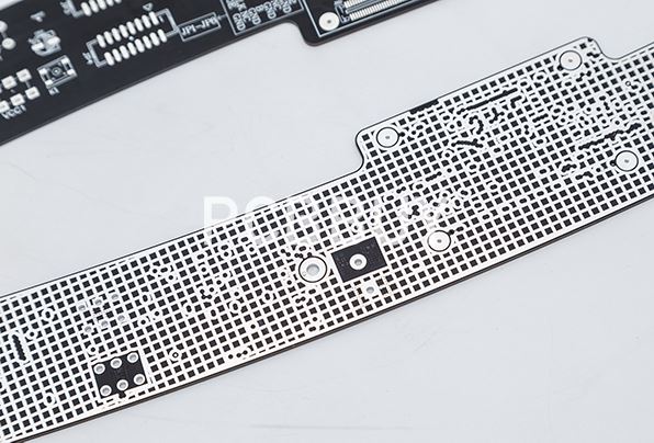
1. Heat Conduction in PCB: During processing, especially during use, printed circuit boards generate significant heat, causing a localized "heat island" effect. This creates substantial internal stress within the board, damaging its internal structure and affecting the performance of electronic products, becoming a major factor in failure. Since the thermal conductivity of metal is higher than that of the PCB dielectric layer, adding a metal plate (on the surface, inside, or both) to the PCB creates a "cold finger" effect. This forms a rapid heat transfer channel within the PCB, lowering the overall board temperature and quickly equalizing it, thus reducing internal stress. Practical evidence shows that products using metal substrates can lower the overall board temperature by 30-50°C compared to organic substrates of the same specification in high-heat environments.
2. Providing Rigidity and Controlling the Coefficient of Thermal Expansion (CTE): The electronic components mounted on PCBs are typically attached via soldering or surface mounting, necessitating a rigid support, which is one of the advantages of rigid-flex PCBs. Metal materials, with their high heat resistance, ductility, high thermal conductivity, and CTE similar to that of copper, meet the need for controlling deformation or size and enhancing reliability during the PCB's operation, when the dielectric layer made of fiberglass and resin may soften or deform due to heat.
3. Acting as a Shield: Metal materials provide superior electromagnetic shielding compared to organic synthetic resins. PCBs in electronic devices are exposed to numerous signal interferences from all directions in the atmosphere, affecting internal signal transmission and the reliability of received signals. Adding a metal layer on the surface or inside the PCB acts as a shield, significantly improving signal transmission or reception integrity. Additionally, the metal substrate can serve as a grounding layer, further enhancing product quality.
Conductive Layer (Copper Foil Layer) Performance in Metal Core Substrates
The conductive layer of metal core substrates is etched from the copper foil layer of the copper-clad laminate. Therefore, the performance of the copper foil in the metal core copper-clad laminate directly affects the performance of the metal core PCB. To enhance the bonding strength between the copper foil and the insulating layer, the back of the copper foil undergoes chemical oxidation, zinc plating, and brass plating processes. These procedures aim to increase peel strength and insulation properties. The typical thicknesses of copper foil layers are 17.5 µm, 35 µm, 75 µm, and 140 µm. In aluminum-based PCBs used in communication power supplies, the commonly used copper layer thickness is 140 µm.
Reference
He Wei, PCB Basic Electrical Information Science and Technology, China Machine Press,322-326
Industry Category


