What Are the Working Logistics of HASL in the PCB Industry?
By:PCBBUY 10/26/2024 16:22
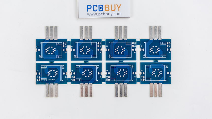
Hot Air Solder Leveling (HASL) is a prominent surface finish technology utilized in the PCB (Printed Circuit Board) industry. Its primary purpose is to create a reliable and solderable surface on PCBs, which is critical for ensuring the longevity and functionality of electronic devices. This article explores the intricate logistics of the HASL process, covering its fundamental principles, operational steps, advantages, disadvantages, and the technologies involved. By understanding these elements, manufacturers can make informed decisions about the most suitable surface finishes for their products.
How to Understand HASL?
Definition of HASL
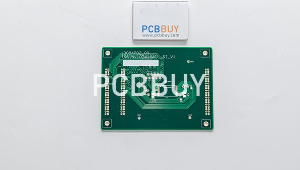
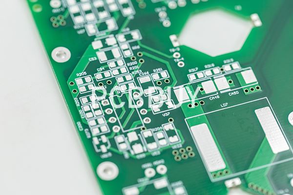
Hot Air Solder Leveling (HASL) is a process that involves coating the exposed copper surfaces of a PCB with a thin layer of solder. This finish not only protects the copper from oxidation but also ensures that the PCB is ready for the soldering of electronic components.
The Principle of HASL
The HASL process is based on the principle of soldering, where molten solder is applied to a PCB to create a robust and solderable surface. The following chemical reaction typically occurs during the soldering process:
Cu + Sn→Cu6Sn5
In this reaction, copper (Cu) from the PCB interacts with tin (Sn) from the solder, forming a copper-tin intermetallic compound that enhances the bond strength of the solder joint.
What Are The Logistics of the HASL Process?
Equipment Required for HASL
The HASL process involves several specialized pieces of equipment, including:
1. Solder Bath: This is a heated tank that holds molten solder, typically maintained at temperatures around 250°C (482°F).
2. Hot Air Leveling System: This apparatus utilizes jets of hot air to remove excess solder from the PCB, ensuring a uniform coating.
3. Conveyor System: A conveyor transports PCBs through various stages of the HASL process.
4. Cooling Station: After solder application, PCBs are cooled to solidify the solder.
What Is Step-by-Step Process Flow?
The HASL process consists of several key steps:
1. Loading the PCBs: The PCBs are placed onto the conveyor system for processing.
2. Cleaning: Before soldering, PCBs undergo a thorough cleaning process to eliminate any contaminants, such as oils, dust, or oxidation.
3. Solder Dipping: The cleaned PCBs are immersed in the molten solder bath. The solder adheres to the exposed copper surfaces.
4. Hot Air Leveling: After the solder dip, the PCBs are subjected to hot air jets that remove excess solder, leaving behind a thin, even coating.
5. Cooling: The PCBs are cooled, allowing the solder to solidify.
6. Inspection and Quality Control: Post-cooling, automated inspection systems assess solder thickness and adhesion quality.
What Are Quality Control Measures?
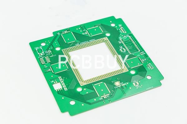
Quality control is critical in the HASL process to ensure the reliability of solder joints. Common quality control measures include:
Thickness Measurement: Techniques like X-ray fluorescence are used to measure solder thickness accurately.
Adhesion Tests: These tests evaluate the bond strength of the solder coating to the PCB surface.
Visual Inspection: Automated systems conduct visual inspections to detect defects, such as solder bridging or uneven coating.
What Are Advantages of HASL?
Cost-Effectiveness
One of the primary advantages of HASL is its cost-effectiveness. Compared to other surface finishes, HASL is generally less expensive, making it an attractive option for high-volume PCB production.
Excellent Solderability
HASL provides excellent solderability, ensuring reliable connections between components and the PCB. This characteristic is crucial for the performance of electronic devices.
Broad Compatibility
HASL is compatible with various PCB manufacturing processes, including both through-hole and surface mount technologies.
What Are Disadvantages of HASL?
Environmental Concerns
Traditional HASL uses lead-based solder, raising environmental concerns. However, many manufacturers now offer lead-free HASL alternatives to address these issues.
Thickness Variability
The solder thickness can vary across the PCB surface, which may impact solder joint reliability. Consistency in solder thickness is essential for ensuring quality.
Oxidation Issues
If PCBs are exposed to air for prolonged periods, the solder surface can oxidize, which may compromise solderability.
What Are Applications of HASL?
HASL is commonly used across various sectors, including:
Consumer Electronics: Commonly found in smartphones, tablets, and laptops.
Automotive Electronics: Due to its reliability, HASL is widely used in automotive PCBs.
Industrial Equipment: Applied in control systems and manufacturing machinery.
What Is Comparative Analysis of Surface Finishes?
To better understand where HASL stands among other surface finishes, the following comparison provides insights into various options available in the PCB industry:
|
Surface Finish |
Cost |
Solderability |
Lead-Free Option |
Thickness Control |
|
HASL |
Low |
Excellent |
Yes |
Moderate |
|
ENIG |
Moderate |
Excellent |
Yes |
Good |
|
OSP |
Low |
Good |
Yes |
Excellent |
|
Immersion Gold |
High |
Excellent |
Yes |
Good |
Conclusion
Hot Air Solder Leveling (HASL) remains a popular choice for PCB surface finishing due to its cost-effectiveness and reliable solderability. Understanding the logistics of this process, from equipment to quality control, is essential for manufacturers aiming to produce high-quality PCBs. As technology advances, the PCB industry may continue to evolve towards more environmentally friendly alternatives, yet HASL will likely maintain its significance in the market.
References
1. IPC-2221: Generic Standard on Printed Board Design.
2. "Surface Finishes for PCBs: A Comparison" - PCB Design Magazine.
3. "Hot Air Solder Leveling Process Overview" - Journal of Electronic Manufacturing.
4. ASTM B733 - Standard Specification for Electrodeposited Coatings of Nickel.
5. "Environmental Impact of Soldering Processes" - Journal of Environmental Engineering.
Industry Category


