What Causes A Cold Solder Joint in PCB Manufacturing?
By:PCBBUY 03/25/2022 10:16

This failure is more prominent in Land Grid Array (LGA) and Quad Flat No Lead (QFN) packages, as they often do not have solderable side terminations or the component manufacturing process has made them poorly solderable. Often, a lack of protective coating of tin on the surface of copper lead frame is the cause of poor solderability of the edge termination.
In this passage, we are providing all the professional knowledge of solder joint in PCB manufacturing. If you are searching for the information about solder joint in PCB, please check and read the content below for more.
What are the common failures of solder joint?
· Open joints
· Incomplete solder coverage
· Solderability failure
· Floating LGA
· Component Damage
· Solder skip
· Solder balls
· Fillet lifting in through holes
· Non-Coalescence of paste
· Popcorning/cracking
· Surface corrosion and copper dendrites
· Tin whiskers
· Incomplete reflow of pin in hole
· Insulation contamination
· Pad lifting
· Non-reflow of paste
· PCB Delamination
· Incomplete Wetting
· Solder Wicking
· Outgassing and Blowholes
OPEN JOINTS
This is the most common type of defect especially found under POP packages, where two or more Chip Scale Packages (CSP) or Ball Grid Array (BGA) components are placed one on top of the other and reflow soldered. Package warping is one of the main reasons for such open solder connections, which can cause one or multiple open connections.
Poor solderability may be another reason for the formation of open joints. Paste deposit extending too far under the body of the component may be another reason. The excess solder can lift the component and its lead above the surface of the solder paste as it reflows before allowing the lead to wet, leaving the joint open.

INCOMPLETE SOLDER COVERAGE
Also Read: Preventing Corrosion in Printed Circuit Boards
Increased temperatures in lead-free processes can cause solder to solidify prematurely as the inner layers lose heat. This results in solder joints with a reduced hole filling.
SOLDERABILITY FAILURE
This failure is more prominent in Land Grid Array (LGA) and Quad Flat No Lead (QFN) packages, as they often do not have solderable side terminations or the component manufacturing process has made them poorly solderable. Often, a lack of protective coating of tin on the surface of copper lead frame is the cause of poor solderability of the edge termination. Although IPC 610 does not require side terminations to be solderable, customers prefer to see a joint. Additionally, the presence of solder on the edge termination helps Automatic Optical Inspection.
FLOATING LGA
During reflow, Land Grid Array (LGA) packages may lift, resulting in open solder joints. This is mostly caused by excess solder paste under the center pad of the package causing the part to float on the surface of molten solder. This is easily corrected by changing the stencil design. The aperture for the center pad should be only 50-60% of the area of the pad. If possible, splitting up the area of the pad with 4-9 equally spaced apertures also helps.
COMPONENT DAMAGE
Passing through the solder reflow process can be a tough time for Moisture Sensitive Devices (MSD), unless they are packaged properly to prevent them from mechanical damage from handling or cracking. Exposing such MSDs to high levels of humidity may lead to cracking of the component body or pop corning during reflow.
SOLDER SKIP
This is a common defect in wave soldering caused by incorrect wave height. Usually, there is no solder on the pad or on the termination. However, process issues such as flux gassing should also be investigated along with wave height.
SOLDER BALLS
This is a typical result of using paste to rework parts such as BGA, where excessive paste turned into a ball during reflow. The presence of the ball reduces the insulation separation distance below the required minimum. Solder balls can be removed with a high-pressure airline directed with care, but require a follow-up inspection with optical or x-ray.
FILLET LIFTING IN THROUGH HOLES
Lead-free soldering often causes fillet lifting in through-hole component leads. Sometimes, along with the fillet, the pad may be separated from the laminate as well. However, in most cases, this failure does not lead to a joint failure or an electrical failure. The main reason for this type of failure is related to the expansion and contraction the PCB undergoes during soldering and the solidification of lead-free materials. IPC 610D inspection criteria covers this process issue.

NON-COALESCENCE OF PASTE
With component sizes shrinking, small paste deposits often do not fully reflow in air, and this is very common with lead-free solder paste when operators use a traditional soak profile. The solder paste turns into balls that do not fully reflow into the bulk of the solder joint. This defect is common in 0201 and 01005 chip components during convection reflow. As the small deposit of solder paste is exposed for a long period of elevated temperature during the lead-free profile, it reduces the performance of the flux in the paste. The inert atmosphere in vapor-phase soldering does not allow this to happen.
POPCORNING/CRACKING OF COMPONENTS
Incorrect specification or use of the component can lead to its popcorning or cracking during the elevated temperature of lead-free solder reflow. This can be corroborated with the maximum soldering temperature and duration suggested by the manufacturer of the component.
Flux and Oxidation
pcb assemblyMost PCB assemblers are not chemists, but it helps to understand some basic chemistry to understand the value of solder flux. During soldering, the molten solder forms a hot eutectic, and the molten solder can easily react with oxygen to form oxides. Metal oxides tend to have low mechanical strength compared to their pure metal counterpart.

The use of flux is intended to suppress oxidation, as well as to draw solder onto the intended area during assembly. Flux provides another benefit in that it helps clean the area of any oily residues. The correct flux and a sufficient amount of flux must be matched to the correct type of solder during PCB assembly.
Temperature and Wetting
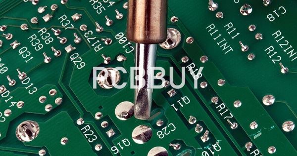
When solder is heated, the mix of metals forms a hot eutectic and wets the surface of a pad (for SMT components) or via (for through-hole components). The surface tension of the molten solder during wetting will draw the solder into a convex “fillet” shape at the edge of the component, and the solder will cool once the heat source is removed. However, if the solder temperature is too low during heating, the solder will not form a thoroughly-mixed eutectic and will solidify as a cold joint.
A cold joint has dull, pockmarked surface and low strength due to insufficient mixing of the eutectic. The lack of heat on the joint during soldering can result from one of two possible reasons:
Insufficient iron temperature: The soldering iron was too cool for the type of solder being used.
Excess heat dissipation: Too much heat was removed from the solder point, which decreased the temperature of the eutectic during soldering.
Industry Category


