What Causes Solder Bridging & How to Prevent it in PCB Manufacturing?
By:PCBBUY 03/11/2022 10:00

The issue can be aggravated if the solder paste mask is absent or only covers a narrow area between the pads. This enables the solder paste to rest on the substrate, which causes solder bridges to easily form.
Sometimes, solder bridging is caused by stencil thickness, which affects the volume of solder paste applied onto the pad. A thicker stencil will lead to more solder paste on the pads, which may cause the paste to overflow from one pad to another. If you are searching for more information about solder bridging in PCB manufacturing, please check and read the content in this passage.
What the causes are of solder bridging in PCB manufacturing?
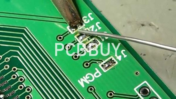
Solder bridging can occur during printed circuit board assembly for a variety of reasons. Here are some of the top causes:
Component Placement
The position of parts on the board, both during design and then again during manufacturing, can have a big impact on how the board is soldered:
Component footprints need to be located on the board during PCB design for the assembly soldering process. For instance, wave soldered boards need to have surface mount discrete parts placed perpendicular to the direction of the board, traveling through the wave so their pins solder evenly.
During assembly, the physical parts must be placed correctly on their footprints to avoid uneven soldering due to the wrong lead to pad size relationship.
Incorrect Solder Mask Definition
Solder mask is designed to prevent solder from bridging between pads, but if it isn’t defined correctly it may not provide the protection expected of it:
· Surface mount pads that are larger than they should be could end up being too close to each other for sufficient solder mask coverage between them.
· Solder mask shapes in a pad that are defined larger than they should be may not provide enough solder mask coverage to protect the pad from bridging.
· Fine pitch pads on large pin-count devices can cause problems if the solder mask is defined too narrowly or missing altogether between the pads.
· If the solder mask is insufficiently applied on the board during assembly, it can also leave the spaces between pads unprotected.
Incorrect solder paste stencil specifications
Solder paste is often applied with a stencil. If the stencil is made incorrectly, the solder paste will not be applied in the correct proportions and could easily bridge from one pad to another:
· If the surface mount pads on the board are smaller than what they should be, the solder stencil apertures for those pads will deposit too much paste on the pad.
· If the stencil apertures were made too large for their associated pads, then again, too much solder paste will be applied.
· If the stencil itself is too thick, then unnecessary amounts of solder will be applied to each pad.

What are the considerations of solder bridging in PCB manufacturing?
Tombstone- This refers to a condition where a component is lifted up during wave soldering and resembles a tombstone. This is often caused on account of having an incorrect lead length or using components that have different solderability requirements.
Excess Solder- As the name suggests, this results from an excess build up of solder. This could be on account of a fast conveyor belt or an incorrect lead length to pad ratio.
Solder Balling- This is a result of solder attaching itself to the Printed Circuit Board during wave soldering. Solder balling can result on account of the temperature being too high or on account of the solder splashing back onto the board.
De-wetting and non-wetting- De-wetting refers to when the molten solder covers a pad and retreats, leaving behind a mound of solder. Non-wetting on the other hand refers to the solder leaving behind exposed copper. This is often on account of the fact that the flux needs to be changed or that the brass components haven’t been plated well.
Lifted Pads- This is known to occur when a soldered component needs to be removed and results in the pad being lifted from the PCB. Lifted pads are often a result of an overworked pad joint or even an uneven layer of copper plating.
Pin holes and blow holes- These are caused on account of excess moisture in the board or even poor copper plating.
Irrespective of what solder bridging is on account of, the fact is that it can pose a host of problems. While we cannot ensure that solder bridging never occurs, there are certainly some key measures that can be taken to reduce the risk of soldering significantly. Check out the complete guide on how Solder Bridges becoming a major challenge during PCB assembly.
Industry Category


