What Is A Through Hole PCB and What Are the Features?
By:PCBBUY 04/26/2022 11:18

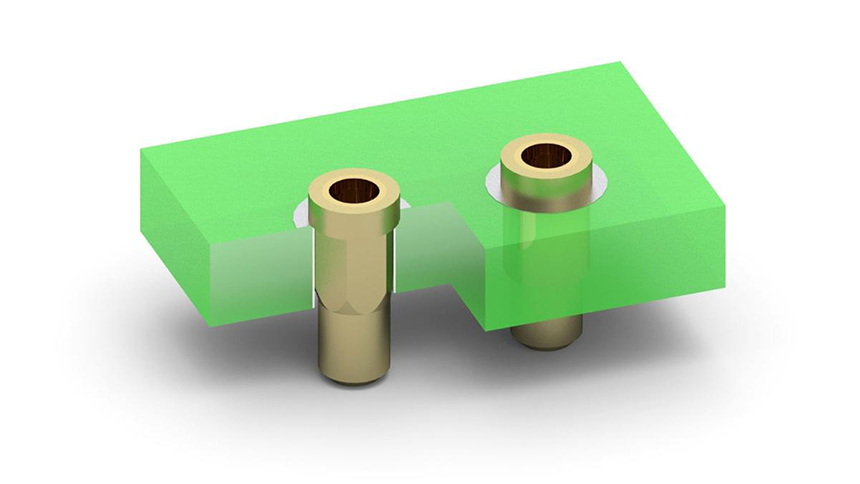
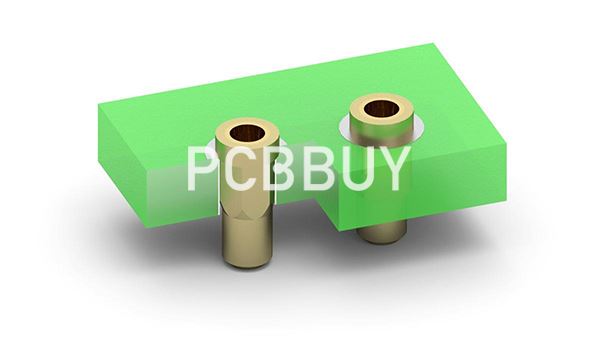
Through-hole technology, also spelled “thru-hole”, refers to the mounting scheme used for electronic components that involves the use of leads on the components that are inserted into holes drilled in PCBs and soldered to pads on the opposite side either by manual assembly (hand placement) or by the use of automated insertion mount machines.
Through-hole technology almost completely replaced earlier electronics assembly techniques such as wire wrapping. From the second generation of computers in the 1950s until surface-mount-technology (SMT) became popular in the late 1980s, every component on a typical PCB was a through-hole component.
If you are curious about the process of Through Hole soldering on PCB, please check and read the content below for more information. You may find all the details about Through Hole soldering on PCB.

What are the benefits of Through Hole on PCB?
Benefits of Through Hole Technology
Soldering through hole components is relatively old technology. However, it is still a useful method. Through holes soldering makes the bond between the printed circuit board and the through hole components very strong. Thus, through hole soldering is an appropriate method for electronic equipment that will be subjected to mechanical stress or excess heat. Transformers are an example of such equipment.
Also, it is easy to maneuver through hole PCBs. This makes them suitable for testing and manufacturing prototypes. In addition, the holes are well spaced which allows through hole soldering by hand.
THT soldering could be cost-effective. When working with through hole PCBs you do not have to generate a different solder template every time you alter the PCB. This could help save a lot of money especially if the design undergoes a couple of spins or more before it is satisfactory. Also, tin-lead solder can be used during THT soldering. This solder is the cheapest exterior metallization.

How to process Through Hole on PCB?
Alkaline cleaning
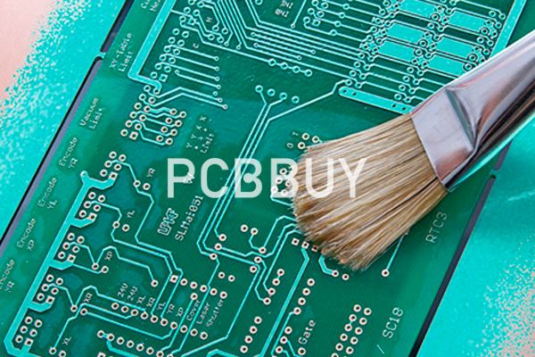
Remove the board oil , fingerprint, oxide, dust in the hole; adjust the negative charge to positive charge for hole wall so that the colloid palladium does well in being adsorb in the post-process; it should be strict with cleaning based on guidance after unoil and test with PTH backlight.
Mircoetching
Removing the oxide of board, and roughening the board, to make sure that there is a good bonding between plated through hole layer and base copper; the new copper foil has a strong active and does well in adsorb the colloid palladium;
Pre-dip
It’s mainly in protecting the palladium slot from being polluted for the bath of pretreatment and extending the shelf life, the main ingredients of pre-dip is the same as palladium slot but except the palladium chloride, and pre-dip plays an effective role in wetting the hole wall so that the following activator enter the hole on time to be activating effectively;

What are the features of though hole in PCB?
One cost saving for a through-hole PCB is that there is no need to generate a new solder stencil each time the PCB undergoes a revision change. This can save hundreds of dollars on a design which goes through two or three spins before it is deemed to be functional. It is also unnecessary to set up pick-and-place equipment, or to purchase accompanying reels of SMT components, until the final PCB configuration is working and ready for production.
In-circuit testing after component assembly can often be done manually and in-house for a small batch of boards, thereby eliminating the expense of fixtures or associated setup charges. The final advantage is that it is possible to use tin-lead solder (the least costly surface metalization) when working with through-hole boards. The inherent non-planarity of HASL, which can make placement of fine-pitch surface mounted components difficult, is not an issue on through-hole designs.
Another advantage beyond the avoidance of SMT-related cost adders is that it is possible to evaluate mechanical issues (such as excessive warp and twist) during validation, and to compensate for them during redesign, without causing insurmountable assembly difficulties, as might occur with SMT. This is because warp and twist is not nearly as critical on a hand-assembled PCB as it is on one populated using pick-and-place equipment. A human assembler can simply change their wrist angle to improve the fit of a stubborn component, but an automated machine requires a PCB with a high degree of flatness in order to function properly. Your through-hole prototype can expose design-related mechanical shortcomings before they become costly and time-consuming “line-down” three-way screaming matches between your PCB fabricator, your contract assembler, and yourself.
In summary, when the necessary component types are available in through-hole form, the use of through-hole technology during the development cycle can keep your project on track and can simplify the process of assembling prototype and small-lot projects without paying for third party services. Timelines may be more predictable and controllable with fewer side issues that might delay your product’s critical time-to-market. It may therefore be worth considering at least the temporary use of through-hole components during early development and validation stages, whether you as the end user are a hobbyist, an industry start-up, or an established electronics supplier.
Industry Category


