What Is Annular Ring in the PCB Drilling Process?
By:PCBBUY 12/23/2021 09:16

When you drill a hole into a copper PCB pad, the resulting copper surrounding the hole is what we know as annular rings. It essentially acts as the wall of the drilled via. Your annular ring size will depend on the size of the via and the size of the copper pad’s size.
But what is the purpose of the annular rings? As you may or may not know, PCBs are multi-layered. Your circuit board traces will need to connect to various layers of your PCB. They usually achieve this by reaching a pad which routes them through to another layer by a via. If you are curious about annular ring PCB, please check and read the content below for more information.
Wanna know PCB knowledge? Check and read for more.
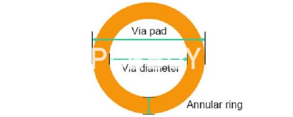
What is the relationship of annular rings and vias?
The via hole must be drilled at the absolute center of the pad to form the annular ring or the minimum width of the ring must be above the specified value. Misregistration of the via with respect to the land can lead to marginal interconnections that exhibit increased resistance and perhaps lead to reliability problems.
The smallest clearance (−1 mil), included to verify that the proper hole size was drilled, is intentionally designed to fail. The probability of breakout decreases from 98 percent for the 2 mils designed clearance to zero for the 6 and 7 mil clearances. If the breakout is not allowed, then designs fabricated by the supplier in this example would require rings of 6 mils or larger for the microvias. By designing 5 mil annular rings, the data estimate that 5 percent of the microvias will exhibit breakout.
Why size is important to PCB annular ring?
The width of the ring should be sufficiently thick to allow reliable electrical connection with via. The minimum length of the ring should be greater than or equal to the specified width for the design. A dimension that is less than the value specified in the design can interfere with the attachment of the component. It can also lead to pad breakout (zero annular ring), a condition associated with the region where the circuit enters the pad. This can reduce the current-carrying capacity of the circuit.
· Common annular ring issues
· Undesired annular ring
· Tangency
· Breakout
What are the considerations of PCB annular ring design?
When we look at the accumulated process values we will divide the tolerance in half. This can be halved since we split the error across the production panels. So if we add everything together for a high layer count single lamination cycle the process allowance can be .0045” for tangency. If the job has multiple lamination cycles, the allowance for tangency would be .006” for the final drill.
If you are considering Class 3 then the annular ring value would increase an additional .001” – so for a single lamination cycle we typically ask for a .006” annular ring. For multiple lamination cycles we will allow a .006” annular on the first sub-lamination cycle but will ask for .007” annular ring on the following lamination cycles.
The last item for designers to consider is the drill size the fabricator actually drills with. To answer this question, it would be beneficial if the designer had two rules. One rule for plated vias in which the finished hole size does not matter and a second rule for component hole sizes that typically have a lead in finished plated hole. Component holes should list the finished hole size and the allowed tolerance.
Vias should be stated as vias and that the finished hole size may finish to any size less than the specified drill size. Most designs list the via size that matches the actual drill bit size the fabricator should use. Using the actual drill bit size will provide the correct annular ring and a “safe” keep back distance between a drill bit and a different net. To clearly convey that a particular drill is a via, the designer should use the following tolerance in the drill chart. This examples uses a .010” via size.
What is the application of PCB annular ring?
Annular rings are integral elements of a PCB as they create room for solid electrical connections on a board. Without these rings, you will be unable to create reliable connections on your PCB. Issues related to annular rings are problematic and significantly affect the trace continuity and the functionality of the entire board.
Unfortunately, some designers ignore the importance of annular rings by creating distorted shapes. When designing annular rings, you should be accurate to avoid drilling off the mark. By doing so, you will eliminate the annular ring tangency.
Why to process PCB annular ring?
When using the smallest possible drill and pad, there is a chance that one or more holes will slightly overlap the edge of its pad [Figure 1]. Breakout is rare, but when PCB designers push the limits, this can happen to the smallest drills and pads.
The problem occurs when the breakout is in the same direction as a trace entering the pad [Figure 2]. When the hole overlaps the trace, there is a chance of an open circuit or a fragile connection [Figure 3] that could crack later. This decreases PCB yield, increases cost, and lowers reliability. This problem can be helped by using teardrops [Figure 4]. This pad shape extends the size of the pad but only in the direction of the trace. This acts as a larger pad but does not use any additional layout space. A teardrop pad can help push the process limits for the smallest possible annular ring without increasing cost.
Some PCB design tools don’t have the capability to add teardrops. In this case, the PCB manufacturer might be able to add them to your design. The result is a BGA layout with dog-bone shapes. The amount of copper added to make a teardrop dog-bone is small. Teardrops are often barely visible to the naked eye.
Industry Category


