What Is Component Orientation in PCB Manufacturing?
By:PCBBUY 03/19/2022 09:53

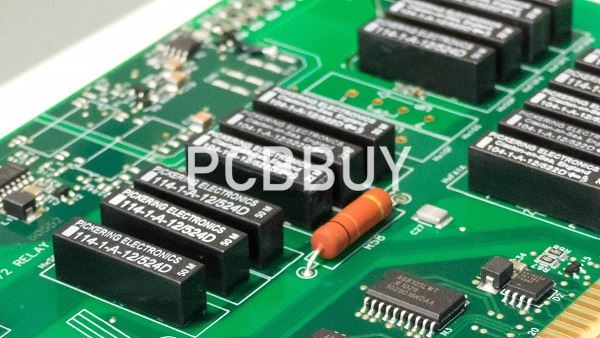
At one time, a circuit board could be laid out with its parts arranged aesthetically and it would perform just as well. However, that is no longer the case—today, PCB quote components must be placed in specific partitions according to their function for optimum performance. They also have to be oriented correctly to satisfy the needs of the signal or power circuitry they are servicing.
In this passage, we are going to provide you all the details about component orientation in PCB. If you are searching for the information, please check and read the content below in this passage.
What are general component placement and spacing?
Before going into the specifics of component placement and orientation, there are several general guidelines to keep in mind:
· Orient similar components in the same direction.
· Avoid placing components on the solder side of a board.
· Try to place all your SMT components on the same side of the board, and all the through-hole components (if mixed) on the top side of the board.
· When you have mixed technology components (SMT and PTH), manufacturers might require an extra process to epoxy the bottom components.
· You should terminate all lands with only one trace.
· When you specify a chip under a device, this can make inspections, rework, and test more difficult.
· All components used on the wave solder sides of an assembly should first be approved by your manufacturer for immersion in a solder bath.
What are the considerations of component orientation in PCB?
There are three primary goals that your PCB contract manufacturer will focus on when they review your design for manufacturability:
· Standardization: By making sure that your PCB design will fit into a standard assembly process, your CM can reduce the labor and time involved, which lowers your cost.
· Assembly problems: By eliminating known potential assembly issues, your CM will improve production yields and once again pass on cost savings to you.
· Quality: By identifying and replacing parts or materials that could be potentially defective from the assembly process, your CM can once again improve yields.
· During the DFM review, one of the details of your PCB that will be looked at to achieve these goals is component orientation. The rotation of parts on a PCB can have a great effect on its manufacturability, starting with the soldering process.
For boards that are waved soldered, components that are misaligned could cause poor or bad solder joints, leading to intermittent electrical contact, no contact, or even direct shorts. Here are some component orientation considerations to keep in mind for wave soldering:

Surface-mount passive components such as resistors, capacitors, and inductors, should be aligned perpendicular to the direction of the board going through the wave so that both pins get soldered equally.
Larger SMT components should not precede smaller components through the wave. This could cause “shadowing” of the smaller components and reduce the wave’s ability to produce an effective solder joint on the trailing smaller components.
SMT dual inline parts, such as small outline integrated circuits (SOICs) should be placed with their long axis aligned with the wave. Traveling perpendicular to the wave could also produce a shadowing effect on the trailing pins, and cause incomplete or bad solder joints.
Multi-pin parts, such as large through-hole connectors, should be placed so that they travel perpendicular to the wave. This will reduce their chance of creating bad solder joints on the trailing pins.
What is the importance of component orientation PCB?
The success rate of wave soldering circuit boards depends on how well the part placement is optimized for the process. The location and orientation of the parts can make a huge difference in how well the board is soldered. Here are some important points to keep in mind during component placement:

· Surface mount components placed on the back-side of the board will be a problem if they are too close to thru-hole pins. The location of the SMT parts may make it difficult to fashion the fixture correctly which could block the thru-hole pins from the full force of the solder wave. This will result in poor solder connections on those thru-hole pins.
· Large thru-hole connectors with multiple pins need to be placed so that they travel perpendicular to the wave. The more closely placed pins there are in a line that goes through the wave, the more likely that the trailing pins will not be soldered as well.
· Small individual discrete surface mount components should also travel through the wave perpendicular so that both pins get soldered at the same time. This requires that the designer knows which direction the board will be traveling through the wave before the layout begins.
· When placing surface mount components to be wave soldered, avoid placing smaller components behind larger ones in the direction of the wave. This could result in the larger components shadowing the smaller ones and creating a poor solder joint.
· Multi-pin SMT parts such as ICs can be wave soldered, but they should be placed in line with the direction of the wave to avoid shadowing the trailing pins.
· Be careful to not create land pattern pad shapes too large as this could cause solder bridging between them. It is always best to follow IPC specifications when creating your PCB footprints.
· Remember that the height of the wave has its limits, so taller components may not allow for that side of the board to go through wave solder.
Industry Category


