What Is Copper Thieving in PCB Manufacturing and How to Process?
By:PCBBUY 09/27/2022 15:13

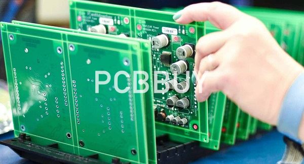
A PCB are kept as solid copper until the drilling and plating processes have been completed to provide a path for the plating current needed to plate the copper in the holes. There are two similar terms used in PCB design; copper balancing and copper thieving. Although they are often used interchangeably, there are some important distinctions between the two.
Copper Thieving is just a fancy way of saying that small copper circles, squares or even a solid copper plane will be added to larger blank spaces to even out the copper distribution across a copper layer.
If you are searching for more information of copper thieving in PCB manufacturing, please check and read the content to learn more about copper thieving in PCB manufacturing.
Why to use copper thieving in PCB manufacturing?
The reaction rate of any etching process is limited by local current densities, access of the reactants into the reaction area and clearance of the reaction products away from the reaction area. Since board etching is essentially a planar or two dimensional process this places further limits on etching performance with reactant delivery and reaction products actively interfering with each other for access to the surface.
While always present in processes, where the problem arises is in the differential etch rates across the board. This can cause thin traces to be etched at a different rate than wider traces. For example, etching a relief from around a fine trace within a background of a ground plane is very different in loading than etching a thin trace with no background ground plane.
This can be corrected for by ensuring that in the design the pattern density remains fairly constant per unit area across the board. Thieving is one way to do this. Some manufacturers will actually place sacrificial elements within the tanks and along side the board to ensure proper yield of different line thicknesses.

What are the plating operations of copper thieving in PCB?
Outer Layer Plating
Outer layer plating is done to deposit copper in the vias and component lead holes so that connections are formed from one side of the PCB to the other. It’s also done to make the connections to signals and planes on inner layers. The two outside layers of a PCB are kept as solid copper until the drilling and plating processes have been completed to provide a path for the plating current needed to plate the copper in the holes.
Panel Plating
In the early days of PCB manufacturing, the entire panel on which a PCB was formed would be immersed in the plating bath after the holes had been drilled and the burs and debris were cleaned away. This is referred to as panel plating. The challenge with panel plating is that copper is plated all over the surface even in those areas where no traces or pads will be placed after the etching process. This results in two issues:
The etching of the unwanted copper has to go through the copper plated onto the outer surface as well as the original copper on the outer layer. This requires the use of more chemicals and also takes more time.
As the etching goes down through the copper it also etches sideways resulting in less accurate trace width control. This led to the pattern plating process described below.

Pattern Plating
Pattern plating is a process where copper is plated up only on those features that will remain behind after the outer layers are finally etched. Usually, the features included are all of the plated through holes, the traces and the component mounting pads. This process is accomplished by applying a plating resist to the two outside layers after drilling has been completed. This plating resist is photosensitive and is exposed to a light that solidifies the resist in areas that are not to be plated. This unexposed resist is washed away, and the areas that must be plated are left exposed. Plating is the next step that takes place.
The problem with pattern plating is that if the features on the outside layers are not evenly distributed across the surface. The plating currents will also not be evenly distributed and some features, such as vias and connector holes, will plate less heavily or uniformly than the others that are spaced farther apart. When there is a need for very uniform plating, such as in the holes of a press-fit connector, as shown in Figure 2, something must be done to spread the plating current evenly across the entire surface. This is where thieving comes into play.

How can you apply copper thieving to PCB design?
The manufacturing of the copper traces of your board, whether on the surface or for internal layers, is done by etching, one of the major PCB manufacturing steps. Layer fabrication begins with a laminate sheet that is completely covered by copper. Etching is the process of removing excess copper from traces and other areas, such as component pads and annular rings for vias, using an ammonia-based solution.
Typically, these sheets begin with preset copper thicknesses. This thickness can be etched down, decreased, or plated up, increased, to the desired specification. Due to the manufacturing process for the sheets, the surface has a degree of roughness that helps with bonding to the dielectric material. However, this can have an increasingly adverse effect on signal integrity at higher frequencies. At frequencies above 100MHz, the skin effect, where current flow is typically near the internal surface of the trace as opposed to through the conductor center, occurs, causing the effective resistance of the trace to increase and oppose current flow.
Traces for plated vias must be added after the holes are drilled. A process for accomplishing this is electrodeposition where the board is placed in an electrolytic solution containing copper ions. A direct current is applied to set up a potential across the via and ions are distributed throughout the via. The distribution of the copper ions throughout the via or the filling determine the quality of signal flow along via traces.
Industry Category


