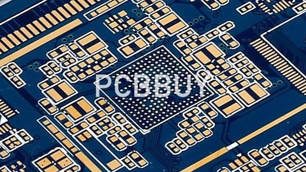
What Is ENIG PCB and What Are the Advantages of it?
By:PCBBUY 12/16/2021 09:41

Despite the higher pricing of ENIG surface finishing, it has a high success rate for producing high-quality products. It holds up under multiple thermal cycles, showcases great solderability and is a suitable option for wire bonding. As the name suggests, it consists of two coating layers — nickel and gold. The nickel protects the base copper layer and enables secure attachment of electrical components, while the gold serves as an anti-corrosion measure for the nickel.
If you are looking for the professional knowledge of ENIG PCB, or get into know the surface finish, please check and read the content in this passage below.
What are the features of ENIG in PCB?
This type of finish involves a two-layer metallic coating; it consists of electroless plating that is covered with a thin layer of immersion gold, the function of the immersion gold is to safeguard the nickel from oxidizing during storage, and the nickel functions more like a barrier to the copper and a surface on which the components are soldered. Recently, due to the advantages provided by ENIG, ENIG is one of a printed circuit board (PCB) industry, the most common types of surface treatment, including a plane, lead-free, suitable for plated through holes (PTH), long shelf life.
In the early stages of ENIG plating, reliability is still unclear, i.e., this type of leaf had dependability problems. This has resulted in the disuniting of the copper pads from the finish. Unlike the hot air solder leveling, the electroless immersion nickel-gold does not uniformly wet. To ensure that the conventional coating provides the proper temperature and concentration, the reducing agent consisting of nickel ions must be renewed.
What are the advantages and disadvantages of ENIG in PCB?
Advantages of ENIG
• Unlike the hot air solder leveling, the electroless nickel immersion gold offers a flat surface
• It is a type of surface finish suitable for plated through holes.
• More like the hot air solder leveling, it provides good storage life
• It has no lead
• This type of surface finish is suitable for use as bottom metal for cob wiring.
• ENIG has an excellent electrical conductivity ability
• The electroless nickel immersion gold is recognized for its capability to prevent oxidation.
Disadvantages of ENIG
• One major challenge is that it is expensive
• Unlike the hot air solder leveling, the ENIG is not re-workable
• The electroless nickel immersion gold is associated with signal loss
• Unlike the HASL, ENIG has a more complicated process.
• ENIG is prone to the black pad, due to its low wielding strength

What is black pad of ENIG in PCB?
In the permutation reaction of ENIG process, if the nickel surface get excessive oxidation reaction, the metal nickel might convert into nickel ions, while the larger gold atoms (radius 144 pm) irregularly deposit to form a coarse and loose arrangement, which means the gold layer might fail to completely cover the nickel layer, allowing the nickel layer to contact with the air, which will finally create nickel rust under the gold layer. This kind of nickel rust will cause soldering failure.
So that another surface finish process called ENEPIG was come up to solve this problem of "black pad", but the cost of ENEPIG is relatively expensive, now it is more suitable for HDI boards, CSP or BGA.
What are the professional considerations of ENIG in PCB?
ENIG process is in line with the environmental protection requirements advocated by many standards worldwide. The lead-free process gives customers ease and assurance in using it. As a chemical process, ENIG ensures a flat surface of gold covering the pads, which allows for better soldering performance and a longer shelf-life. It is especially suitable for modern automated SMT, and also very friendly to BGA soldering. Therefore, PCB with higher precision requirements often opts to use ENIG.
However, the ENIG process also features disadvantages, namely, higher cost and higher process complexity. With consideration of cost, when precision or quality requirement is low, lead-containing or lead-free HASL is often used. In the next episode, we will look at other surface treatment methods for PCB and the differences between them.

How to process ENIG in PCB?
After performing an ENIG finish on PCB, they regularly go into capacity in clusters and anticipate their opportunity to be populated with little parts. These segments will be patched, followed, wire-fortified, sintered, and connected in alternate approaches to the surface mount cushions on the ENIG completed sheets.
If you believe it is ok to open up the ENIG plating and get down to business with the holding, it will be a fun time for you to know the vacuum plasma procedure. Plasma cleaning or plasma treatment is an approach to initiate a surface by designing an artificially viable grouping of particles at the initial not many atomic layers of the materials being fortified.
The job of plasma treatment job in this is to barrage the outside of that ENIG with a gas that adjusts the substance cosmetics of the surface. Attachment of any sort is a compound marvel that requires a specific arrangement of manageable atoms to exist on the two surfaces meeting up to frame the interfacial bond. Vacuum plasma is a typical treatment technique since it can get into amazingly small spaces for exactness substance cleaning. Compound cleaning is the thing that we call getting the synthetic formula of the surface perfectly.
Industry Category


