What Is Edge Plating in PCB &What Is the Process?
By:PCBBUY 03/11/2022 09:47

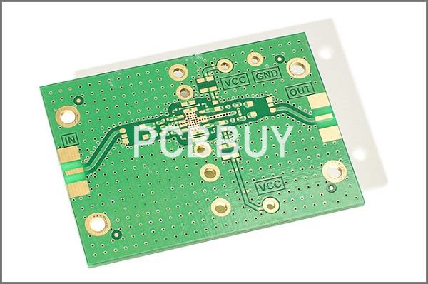
Metalized edging means that the edge of the board must be metalized. English description: Edge plating, border plated, plated contour, side plating, side metal, etc.More electronic products start to minimize the product volume as the goal so that PCB will use electroplated nickel and gold surface treatment(ENIG) technology. In the production process, the gold-plated finger process can achieve the gold-cladding of the solder joints. Still, it is necessary to separately make the lead-through solder joints and the board edges, even though they are removed after gold plating.
In this passage, we are processing all the details of PCB edge plating. If you are searching for more information about PCB edge plating, please check and read all the professional knowledge in this passage.
What is the application of edge plating PCB?
Several industries require edge-plated boards, especially in applications that require better support for connections such as for boards that slide into metal casings. Edge plating has other uses as well as it improves the current-carrying capabilities of the board, provides edge connection and protection, and offers the possibility of edge soldering to improve fabrication.
Although edge plating on printed circuit boards is a simple addition in most cases, fabricators need specialised equipment and trained personnel for the process. Designers must take care that internal power planes do not come up to the edge, and fabricators must make sure there is a gap before they take up edge plating. Designers must make sure there is a band of copper on both edges of the top and bottom side, as the plating will connect to these copper bands.
Now edge plating PCB has been widely used in many industries, particularly in applications that need better support for connections, for example for circuit boards that slide into metal casings. What’s more, edge plating has other benefits as follows:
· Improve the current-carrying capabilities of PCB;
· Offer edge connection and protection;
· Offer the possibility of edge soldering to improve fabrication.
What are the advantages of edge plating in PCB?
But there are more benefits to the performance of your printed board when it’s edge plating.
Thermal Distribution
One of the key benefits of edge plating is its ability to support thermal distribution. Similar to thermal vias, when components become overheated, they are more likely to fail, causing potentially critical damage to the board itself. As customers design circuit boards with more capabilities, using more components tightly packed onto smaller boards, effective thermal distribution becomes essential to channel excessive heat away from temperature-sensitive components. Without the ability to escape, the heat will compromise the performance and reliability of the board.
Signal Integrity
Edge plating can also improve signal integrity. Signal integrity is becoming more important as PCB boards are becoming more complex, demanding faster connections and more complex layouts. Plating on PCB edge is fairly straight forward process in terms of the equipment required, though the process sequence can vary.

What is the process of edge plating in PCB?
Drilling -> Milling Metal Slot -> Get Rid of Dirt -> Copper Electroless
The outer contours, to be metallized, must be milled before through-hole plating process, as the metallization of the edges take place during this fabrication step. After the deposition of copper, the intended surface finish is finally applied to the edges.
Fabrication Issues:
Copper Peeling -Plating over a large substrate surface can lead to the plated copper peeling due to a lack of adhesion strength. We address this by first roughening the surface through a combination of chemical and other proprietary means. Next, we employ direct metallization, which has a higher copper bond strength, to prepare the surface for plating.
Burrs -Often edge plating, especially on castellation holes, can result in burrs from the final machining process. We apply a modified, proprietary process flow that results in the burrs being polished down to the edge of the feature.
Fab Note:
· The antenna position of the gold pad is too large, affecting customer soldering or signal transmission.
· The inner edge pad is connected to the wires on the board, resulting in a short circuit.
· The stamp hole is designed at the edging groove and must be handled in the 2nd drilling process.
· Through the process-related manufacture of the individual PCBs as a panel, a continuous metallization of the outer edges is not possible. No metallization can be applied where the small panel bridges are located.
· One request, the slideplating metallization can be covered with solder mask.
· When purchasing edge plating boards, you must confirm with your PCB supplier the possibility of manufacturing PCBs with plating process, and extent to which the fabricator can edge plate the PCB. Your Gerber files or fab drawing should indicate in a mechanical layer where they need slideplating, and the surface finish they need on it. Most manufacturers prefer a selective ENIG as the only surface finish suitable for round castellation.
Industry Category


