What Is Footprint in PCB Design in Manufacturing Process for Beginners?
By:PCBBUY 11/20/2021 09:12

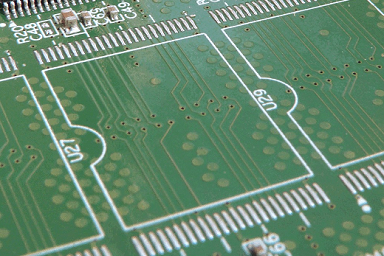
Every component that will appear on a circuit board layout will have a PCB footprint. Whenever you start a new project and jump into a layout, schematic symbols and PCB footprints need to be correct before a single design document is created. The PCB footprint is defined as the physical interface among electronic components or land pattern and printed circuit boards which also comprises of the information of documentation such as reference, polarization mark, and outline.
In this passage, if you are looking for the knowledge for footprint in PCB Design, please check and read the content in this passage for more information.
If you want to order PCB product, please check and custom your order online.

What are the guidelines of PCB footprint?
Components are the most important elements of the board, and pads are the points of connection. If the pad layout fails to accurately identify your component locations or isn’t arranged such that the component can be securely attached, the PCB cannot be assembled. If the pads don’t line up properly with other surface elements like traces and drill holes, your board will not function properly or at all.
Foot print pad layout
Footprint pad guidelines are rules or suggestions that stipulate how pads should be spaced from other pads, other surface elements, drill holes and the board edge. They also define how pads for a single component should be arranged.
Start with exact information
Ensure that you have the correct specifications for the part and the relevant standards, such as IPC-7351, to use as a blueprint.
Build the footprint from the ground up
Start first with the pad information. Whether your tools require a separate pad part, or you must add the pad geometry as an attribute, ensure you have what you need first. Next, create the body outline of the component at the maximum material width. Finally, add silkscreen outlines, reference designators, other attributes, and STEP models to finish the footprint.
What are the challenges of PCB footprint in PCB manufacturing?
Today, the industry is more aware of the need to follow PCB footprint creation guidelines because wasted space isn’t the only thing that can happen if a footprint is created incorrectly. Here are some of the other problems that you might see:
· Incorrect pad sizes: Pads that are too small can cause breakout problems for through-hole parts and bad solder joints for surface mount technology (SMT) parts. Pads that are too large can take up room for trace routing or cause SMT parts to float out of position during soldering.
· Pads that are not spaced correctly: Through-hole pads that are too close together or too far apart can cause problems with component insertion during assembly. SMT pads that are too close or too far from each other can cause insufficient solder joints to be formed, as not enough of the component lead is available for soldering.
· Component outlines that are too small: Footprints that have their body outlines drawn too small will not be able to be assembled using automated production lines. Depending on the severity of the error, the parts may be able to be manually assembled, but that could take extra time and expense. For large errors, the boards may be completely rejected by the manufacturer.
Industry Category


