What Is Gold Fingers in PCB: A Comprehensive Guide to Manufacturing, and Applications
By:PCBBUY 10/23/2024 16:24
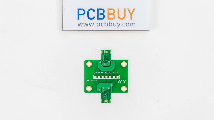
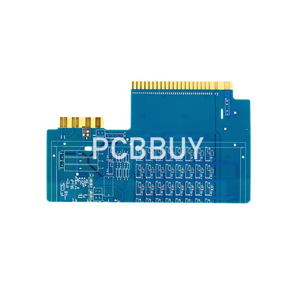
Gold fingers, also known as gold-plated connectors or PCB edge connectors, are crucial components in the design and functionality of printed circuit boards (PCBs). These connectors provide electrical connections between multiple PCBs or between a PCB and other electronic devices. They are used in a wide variety of electronic products, from consumer electronics to industrial machinery, where their superior conductivity, durability, and resistance to wear make them indispensable.
In this comprehensive guide, we will dive deep into the technical aspects of gold fingers in PCB, including their specifications, manufacturing process, chemical principles, and common applications. We will also analyze the importance of gold thickness, the role of the plating process, and offer a comparison of gold finger performance versus other types of PCB connectors.
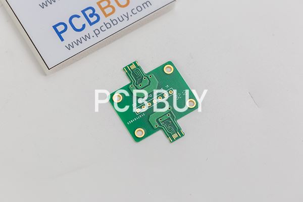
1. What Are Gold Fingers in PCB?
1.1 Definition and Role
Gold fingers are the gold-plated narrow connectors located at the edges of PCBs. These connectors allow electrical signals to flow between the PCB and external components, such as peripheral devices or another PCB. They ensure reliable data transmission and connection integrity, crucial for high-performance applications in the tech industry.
1.2 Why Use Gold?
Gold is widely used for edge connectors due to its excellent electrical conductivity, resistance to corrosion, and superior durability. While gold is expensive, its ability to provide a long-lasting, low-resistance connection makes it the material of choice for high-reliability applications.
1.3 Key Benefits of Gold Fingers
High Conductivity: Gold has a conductivity of 45.2 MS/m (mega siemens per meter), second only to silver among metals, making it an excellent choice for transmitting electrical signals.
Corrosion Resistance: Gold resists oxidation and corrosion, ensuring a long-lasting and reliable connection, even in harsh environments.
Durability: The gold plating on PCB fingers provides mechanical strength and the ability to withstand repeated insertion cycles.
2. Specifications of Gold Fingers
2.1 Thickness of Gold Plating
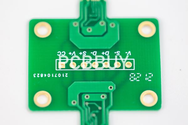
The thickness of the gold plating is a critical parameter in the design of gold fingers. It determines not only the conductivity but also the durability of the connectors. The standard thickness of gold fingers ranges from 0.5 to 3.0 microns, depending on the application and industry standards.
|
Type of Application |
Gold Thickness (Microns) |
|
Consumer Electronics |
0.5 – 1.0 |
|
Industrial Equipment |
1.0 – 2.5 |
|
High-End Applications |
2.5 – 3.0 |
The IPC-4556 standard specifies the requirements for the thickness of gold plating in electronics. Gold plating is typically done over a nickel barrier, which prevents the gold from diffusing into the copper substrate.
2.2 Width and Spacing of Gold Fingers
The dimensions of gold fingers, including their width and the spacing between them, play an important role in determining their performance. The width typically ranges from 0.5 to 3.0 mm, and the spacing between fingers can be as narrow as 1.0 mm.

2.3 Chamfering and Bevel Angle
Gold fingers often feature a beveled edge, known as chamfering, which helps to guide the insertion of the PCB into its socket. The standard bevel angle for gold fingers is 30°, although this can vary based on the design requirements of the PCB.
|
Parameter |
Value |
|
Bevel Angle |
30° – 45° |
|
Width of Gold Finger |
0.5 mm – 3.0 mm |
3. Manufacturing Process of Gold Fingers
The manufacturing process of gold fingers involves several steps, from the initial PCB design to the final gold plating process. This section will explore each of these steps in detail.
3.1 Plating Process
3.1.1 Electroplating
The most common method of gold plating for PCB fingers is electroplating. In this process, a thin layer of gold is deposited onto the copper traces of the PCB by passing an electric current through a gold solution. The chemical reaction involved in electroplating gold can be represented as:
Au3+ + 3e- →Au (s)
This reaction shows how gold ions are reduced to form a solid layer of gold on the PCB. The thickness of the gold layer is controlled by the duration of the electroplating process and the current applied.
3.1.2 Electroless Plating
Another method of plating is electroless plating, which does not require an external power source. Instead, a chemical reduction reaction is used to deposit gold onto the surface of the PCB. This process is less common but can be useful for complex or high-precision applications.
3.2 Surface Preparation
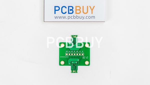
Before the plating process, the PCB surface must be thoroughly cleaned to remove any contaminants that could affect the adhesion of the gold plating. The steps involved include:
Cleaning: The PCB is cleaned with a solution to remove oils, dust, and other impurities.
Etching: A chemical etchant is used to roughen the surface, improving the adhesion of the gold.
Activation: A solution is applied to activate the surface, making it more receptive to the gold plating process.
3.3 Quality Control and Testing
After the gold plating process, several tests are performed to ensure the quality and durability of the gold fingers. These tests include:
Adhesion Testing: Ensures that the gold plating adheres properly to the underlying metal.
Thickness Testing: Confirms that the gold plating meets the specified thickness requirements.
Resistance Testing: Measures the electrical resistance of the gold fingers to ensure optimal conductivity.
4. Electrical and Mechanical Properties of Gold Fingers
4.1 Electrical Properties
The primary function of gold fingers is to provide a reliable electrical connection between two devices. The electrical conductivity of gold plays a crucial role in this process. With a conductivity of 45.2 × 10⁶ S/m, gold is one of the best conductors of electricity, second only to silver.
Gold also has excellent thermal conductivity, which allows it to dissipate heat efficiently. This is important in high-power applications where heat buildup could otherwise damage the PCB.
|
Metal |
Electrical Conductivity (S/m) |
Thermal Conductivity (W/m·K) |
|
Gold |
45.2 × 10⁶ |
318 |
|
Silver |
62.1 × 10⁶ |
429 |
|
Copper |
58.0 × 10⁶ |
401 |
4.2 Mechanical Properties
Gold fingers are subject to mechanical wear and tear, especially in applications where they are frequently inserted and removed from connectors. The hardness of the gold plating is a critical factor in determining how well the gold fingers will withstand mechanical stress.
Gold itself is a relatively soft metal, which is why gold fingers are typically plated over a harder metal, such as nickel. This combination provides both the conductivity of gold and the mechanical strength of nickel.
5. Applications of Gold Fingers in PCB
Gold fingers are used in a wide range of applications, including:
5.1 Consumer Electronics
In consumer electronics, such as smartphones, laptops, and gaming consoles, gold fingers provide a reliable connection between different components. They are essential for ensuring fast data transmission and signal integrity in these devices.
5.2 Telecommunications Equipment
Telecommunications equipment, such as routers, switches, and servers, rely on gold fingers to maintain high-speed connections between components. The durability and conductivity of gold make it an ideal choice for these high-performance applications.
5.3 Industrial and Military Equipment
In industrial and military applications, gold fingers are used in equipment that must withstand harsh environments. The corrosion resistance of gold makes it an ideal material for connectors used in extreme temperatures, humidity, and exposure to chemicals.
Conclusion
Gold fingers are a critical component of PCBs, offering superior conductivity, durability, and corrosion resistance. Their manufacturing process, from surface preparation to gold plating, involves a series of complex steps to ensure that the final product meets the high standards required in today’s electronics industry. As technology continues to evolve, the demand for high-quality, reliable gold fingers will only increase.
References
1. IPC-4556: Standard for Gold Plating in Electronics
2. Smith, J., & Doe, A. (2021). *Advanced PCB Manufacturing Techniques*. New York: TechPress.
3. Wang, T. (2019). "Gold Plating in PCB Applications: A Technical Review," *Journal of PCB Design*, 35(4), 10-25.
4. ASTM B488 - 01(2014), "Standard Specification for Gold for Engineering Uses"
Industry Category


