What Is HDI PCB Design of 5 Tips to Improve the Manufacturing Process?
By:PCBBUY 10/14/2021 09:18

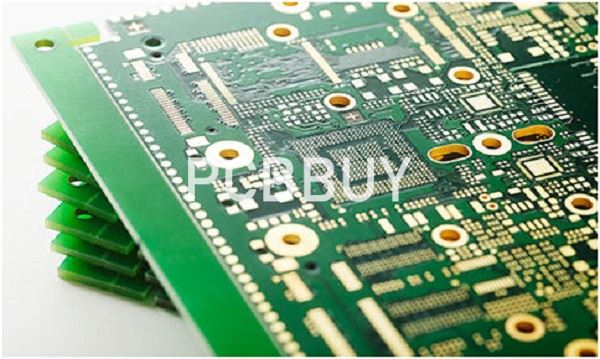
HDI, circuit boards are printed circuit boards with a higher wiring density per unit area than traditional printed circuit boards. In general, HDI PCBs are defined as PCBs with one or all of the following: microvias; blind and buried vias; built-up laminations and high signal performance considerations. At PCB International, we strive to provide the best quality printed circuit boards with wide variety of design characteristics to suit all your project needs.
In this article, you can follow us for more about HDI PCB in the PCB manufacturing process. If you are curious about the HDI PCB information, please check and read the content below for more knowledge.
1. What are the advantages of HDI PCB?
As consumer demands change, so must technology. By using HDI technology, designers now have the option to place more components on both sides of the raw PCB. Multiple via processes, including via in pad and blind via technology, allow designers more PCB real estate to place components that are smaller even closer together. Decreased component size and pitch allow for more I/O in smaller geometries. This means faster transmission of signals and a significant reduction in signal loss and crossing delays.
2. What is the usage of HDI PCB?
A HDI PCB is usually found in complex electronic devices that demand excellent performance while conserving space. Applications include mobile /cellular phones, touch-screen devices, laptop computers, digital cameras, 4/5G network communications, and military applications such as avionics and smart munitions.
Automotive and aerospace industries, where lower weight can mean more efficient operation, have been utilizing HDI PCBs at an increasing rate. Like almost everything else, cars are becoming more connected and computerized. Today’s cars have around 50 microprocessors on board that play a role in engine controls, diagnostics, safety features and other conveniences. Many advanced features such as onboard WiFi and GPS, rearview cameras and backup sensors rely on HDI PCBs. As automotive technology continues to advance, HDI tech will likely play an increasingly important role.
HDI PCBs are also prominently featured in medical devices; advanced electronic medical devices such as equipment for monitoring, imaging, surgical procedures, laboratory analysis etc., incorporate HDI boards. The high-density technology promotes improved performance and smaller, more cost-effective devices, potentially improving the accuracy of monitoring and medical testing.

3. What are the applications of HDI PCB?
Healthcare
The HDI PCB is making an impact on the medical industry. The medical devices are usually HDI since they can fit in small devices like implants and lab and imaging equipment. Medical equipment plays a crucial role in diagnosing diseases and also do provide life support. Ex: Pacemaker, Diagnostic and monitoring facilities.
Automotive
Car manufacturers are extremely attracted to small-sized PCBs since they can save more space in the car. With the launch of futuristic cars from brands like Tesla, the integration of the electronic devices to provide a better driving experience has been the prime focus of the carmakers. Also read, Case Study: PCBs for Automotive Sensors.
Smart phones and tablets
All smart phones are HDI PCBs with ELIC (Every Layer Interconnection) construction. The HDI PCBs are responsible for creating thinner are smaller portable electronic devices.
Wearable technology
With the launch of Apple watch and other wearable devices like VR headsets, HDI is becoming the major stakeholder in the consumer market. The wearable technology is gaining popularity among the young crowd due to its exceptional functionality.
4. How to select material of HDI PCB?
Advanced multilayer technology allows for designers to sequentially add additional pairs of layers to form a multilayer PCB. The use of a laser drill to produce holes in the internal layers allows for plating, imaging and etching prior to pressing. This added process is known as sequential build up.
The application of dry resist to the laminate still uses heated roll method to apply the resist to core material. This older technology process, it is now recommended to preheat the material to a desired temperature prior to the lamination process for HDI printed circuit boards.

5. What is the development of HDI PCB?
HDI printed circuit boards were developed from a need to provide an increased level of computational power and performance in a smaller envelope. This need was driven largely by industries such as telecommunications, where the push to provide smaller and more powerful mobile phones necessitated finding a way to package more electronic circuitry in a smaller, denser package. However, other key drivers in the development of HDI PCBs were the trends in Integrated Circuit (IC) technology that acted as a forcing function to reconsider how printed circuit board layouts and interconnects were designed. Some of these key IC technology trends include:
· The shrinking size of gates
· Reduction in die size
· Reduction in operating voltage levels to control power dissipation
· Higher levels of gate integration (i.e. more transistors per unit area on a die)
· Faster signal rise times (higher operating frequencies and clock rates)
Industry Category


