What Is PCB Etching Process & What is the Importance in PCB Manufacturing?
By:PCBBUY 03/04/2022 09:53

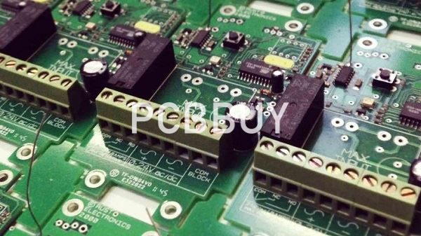
PCB etching is the process of removing copper from a circuit board layer that is not protected by the hardened photoresist by immersing it in a chemical solution. The etching used by industrial circuit board fabricators is broken into two different processes: acidic etching and alkaline.
Do you know the process of the whole process of PCB etching? If you are searching for more information about PCB etching, please check and read the content below.
What are the considerations for etching PCB at home?
You can etch a PCB by yourself, in a lab or even at home, through a simple and inexpensive production process. It makes sense when you wish to produce a single or a very small number of boards and want to avoid manufacturing costs. The etching process is therefore effective for a small workshop. There are however some issues to consider:
· There is a risk of injuries due to the chemicals involved.
· The quality of the results depends on several factors which you won't be able to master completely the first time. This can be somewhat compensated by using good machinery.
· There is the problem of waste disposal. Toxic chemicals require a proper disposal service.
To learn how to etch a PCB, make sure that your PCB design is complete and exported as an etchable PDF or SVG, then follow these instructions.
What are the advantages and disadvantages of etching the PCB?
Advantages of wet PCB etching
· The most important advantage of wet PCB etching is that it can be conducted in a normal atmospheric environment.
· High etching rate
· Low operational cost
· High selectivity: wet etching can be used to etch off a wide range of materials.
· Ease of equipment maintenance
Disadvantages of wet PCB etching
· Inadequate power to etch traces <1μm.
· High use of chemicals
· Creating a significant amount of hazardous chemical waste
· The risk of wafer contamination
· Chemical hazards
· Direct exposure to liquids
· Direct and indirect exposure to fumes

How to process the PCB etching?
There are different ways to produce a mask. We describe two simple methods:
Method A: Direct Toner Transfer
The circuit layout is printed with a laser printer on paper, put face-down on the laminate, and the toner is transfered from the paper to the copper using an iron.
Note that not every paper is suited for this method, including the standard printer paper, but a lot of success stories tell about reused magazin pages. Especially the Reichelt electronic catalogue should produce good results...
The print must be of a very good quality, little mistakes we usually tend to ignore in printed text can result in unusable traces or even cause short circuits. The transfer of the toner is a bit tricky as well. If temperature is too high, the toner gets too liquid and the tracks will blur. If the temperature is too low, the toner won't stick to the copper. After the ironing you can't pull the paper away just like that, without destroying half of the mask. Instead you have to put the laminate with the paper in a water bath and wait a while until you can start to cautiously scrub away the paper. This may take up to half an hour. You might want to check out this tutorial.
Method B: Photo-resistive laminates (Recommended)

The mask is printed on a transparent paper or foil, exposed and developed on the laminate with a UV lamp.
The laminates have a coating that is sensitive to light - by shining a light on them, we can transfer an image of the design to be created onto the board. Where light strikes the board, the coating weakens and creates an area of copper that will be dissolved away by the etching acid.
You will need a UV imaging frame and a photo development kit. Follow these steps:
· Export your PCB layout from Fritzing using File > Export > Etchable PDF/SVG. If you like, you can now edit and enhance the graphics in a graphics software.
· Print the file in highest resolution, first on white paper, and when satisfied, on a transparent paper or foil. Be careful to set the printer options to NOT "scale to fit".
· When printing on foil, use either a special toner or a toner dissolver spray to heighten the density and get the print tone overall even.
· The spray should be used directly after printing, and care should be taken not to cause any drops. After the toner dries, place the foil in the imaging frame, toner side up.
· Peel the protective blue film off the laminate and place it in the imaging frame copper side down, on top of the transparent film. Make sure not to expose the light-sensitive layer to too much light during the development process.
· Close the lid of the imaging frame, set the timer for 4 minutes and press the knob to start the exposure.
· Once the imaging process finishes, place the board in the development tank for 1-2 minutes and shake it once in a while (be careful not to leave it too long, otherwise it will damage the traces).
· Place the board in the rinse tank containing destillated water for a few seconds.
Industry Category


