What Is PCB Thermal Analysis & How to Process it?
By:PCBBUY 03/28/2022 09:56

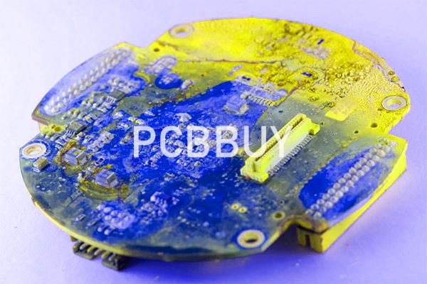
Heat management is crucial for PCB performance, reliability, and longevity. Inadequate heat management may lead to delamination, damage, or device failure (Figure 2). Thermal conductivity plays a vital role in heat management, and thus it is a key parameter for PCB design. The C-Therm Trident thermal conductivity platform is a useful tool in obtaining rapid, precise, and accurate measurements of PCB component thermal conductivity.
If you are looking for more information about PCB Thermal, please check and read the content below for more professional knowledge in this passage.

What is the basic introduction of PCB thermal paste?
The most generic definition for thermal paste is that it is a paste chemically constructed to allow for heat transfer. Its composition is a liquid polymer, that may include urethanes, acrylates, silicones and epoxies. The most typical function for thermal paste is as a filler between two surfaces to provide a solid interface and increase the volume of heat transfer between the surfaces.
With this primary function it may be surprising that the heat transfer rate may range from approximately 3W/(m·K) to 13W/(m·K) for non-metallic pastes, which is far below the 385W/(m·K) for 99% pure copper.
What is the Importance of PCB thermal management?
Current silicon-based components have a junction temperature between about 125°C and 200°C. However, it is necessary to avoid reaching this value, otherwise the residual life of the component will deteriorate rapidly. In fact, it is estimated that an increase in operating temperature of 20°C, due to inefficient thermal management, can reduce component life by up to 50%. High brightness LEDs, for instance, convert over 60% of the absorbed power into heat and therefore require special printed circuit boards capable of handling high temperatures without damaging the components.
The growing popularity of wide bandgap (WBG) semiconductors, such as gallium arsenide (GaN) and silicon carbide (SiC), has allowed components to reach higher operating temperatures than silicon-based technology. This, however, has not eliminated the need for accurate thermal management, capable of evenly distribute the generated heat, avoid the formation of dangerous heat accumulation points (hot spots) and minimizing power losses. Figure 1 shows an electronic circuit subjected to thermal scanning by infrared camera: the red colored parts correspond to the points of greatest heat concentration.

What is the motivation of PCB thermal management?
The main reason for deficiencies of electrical systems beside dust, vibration and humidity is by far the impact of temperature. Therefore an efficient thermal management concept on the PCB is crucial for the reliability of power electronic systems. As an example we take high power LED applications, which are likely to dominate in the next years residential and commercial lighting, signaling and vehicle headlights due to efficiency and extended lifetime. LEDs that range from 500 milliwatts to as much as 10 watts in a single package have become standard, and researchers expect even higher power in the future.
Thermal management is of critical importance for high power LEDs. More than 60% of the electrical power input is converted into heat and built up at the junctions of LED chips due to non-radiative recombination of electron-hole pairs and low light extraction. If that heat is not removed, the LEDs run at high temperature, which not only lowers their efficiency, but also makes the LED more dangerous, less reliable and shortens operating life. Thus, thermal management of high power LEDs is a crucial area of research and development. In this paper results of simulations and measurements of different LED-modules will be shown and should serve as representative of thermal solutions for general high power applications.
Why to process thermal aging test in PCBA?
The purpose of PCB aging tests is to gather data for assessing the long-term reliability of a PCBA that may be placed into continuous operation for over 100,000 hours (at least 20 years). These tests evaluate an entire PCBA, so they tell you the overall reliability of the bare circuit board, its components, solder and mechanical components, and any other materials used in the construction of the PCBA. Obviously, a PCBA cannot be tested for 20 years continuously, so test engineers will perform simulated life testing or other tests to evaluate long-term stability.

With performance requirements and fabrication requirements becoming more complex over time, so has the documentation process used by PCB manufacturers and design teams. With the right design software, a design team can quickly generate their test and fabrication data directly from their PCB layout. Important requirements like the reliability of solder joints, required PCB materials, use of conformal coatings, and a range of test methods can be specified within the project documents and easily shared with manufacturers.
Industry Category


