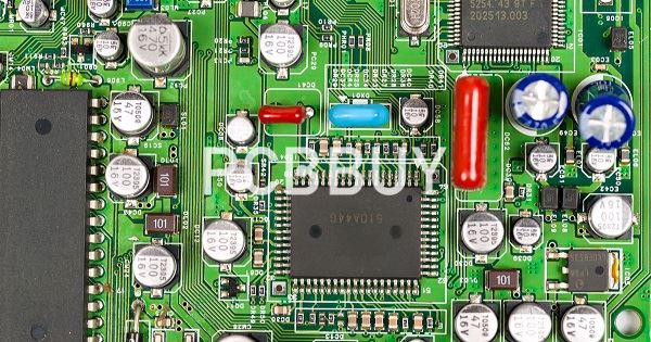
What Is PCB Thermal Analysis for PCB Industry?
By:PCBBUY 01/06/2023 15:46

In high power density PCB, it is difficult to control heat generation. This occurs because there are many channels of traction power at the same time and many elements that depend on the current supply at the same time. High power density PCBS are not necessarily bad designs; Some applications require high power density to perform various functions. In these cases, the efficient use of space is critical, as any crosstalk may quickly cause a thermal peak.
If you are looking for more information about PCB Thermal, please check and read the content below for more professional knowledge in this passage.
What is the Importance of PCB thermal management?
Current silicon-based components have a junction temperature between about 125°C and 200°C. However, it is necessary to avoid reaching this value, otherwise the residual life of the component will deteriorate rapidly. In fact, it is estimated that an increase in operating temperature of 20°C, due to inefficient thermal management, can reduce component life by up to 50%. High brightness LEDs, for instance, convert over 60% of the absorbed power into heat and therefore require special printed circuit boards capable of handling high temperatures without damaging the components.
The growing popularity of wide bandgap (WBG) semiconductors, such as gallium arsenide (GaN) and silicon carbide (SiC), has allowed components to reach higher operating temperatures than silicon-based technology. This, however, has not eliminated the need for accurate thermal management, capable of evenly distribute the generated heat, avoid the formation of dangerous heat accumulation points (hot spots) and minimizing power losses. Figure 1 shows an electronic circuit subjected to thermal scanning by infrared camera: the red colored parts correspond to the points of greatest heat concentration.
What is the defination of PCB thermal paste?
The most generic definition for thermal paste is that it is a paste chemically constructed to allow for heat transfer. Its composition is a liquid polymer, that may include urethanes, acrylates, silicones and epoxies. The most typical function for thermal paste is as a filler between two surfaces to provide a solid interface and increase the volume of heat transfer between the surfaces.
With this primary function it may be surprising that the heat transfer rate may range from approximately 3W/(m·K) to 13W/(m·K) for non-metallic pastes, which is far below the 385W/(m·K) for 99% pure copper.
What is the motivation of PCB thermal management?
The main reason for deficiencies of electrical systems beside dust, vibration and humidity is by far the impact of temperature. Therefore an efficient thermal management concept on the PCB is crucial for the reliability of power electronic systems. As an example we take high power LED applications, which are likely to dominate in the next years residential and commercial lighting, signaling and vehicle headlights due to efficiency and extended lifetime. LEDs that range from 500 milliwatts to as much as 10 watts in a single package have become standard, and researchers expect even higher power in the future.
Thermal management is of critical importance for high power LEDs. More than 60% of the electrical power input is converted into heat and built up at the junctions of LED chips due to non-radiative recombination of electron-hole pairs and low light extraction. If that heat is not removed, the LEDs run at high temperature, which not only lowers their efficiency, but also makes the LED more dangerous, less reliable and shortens operating life. Thus, thermal management of high power LEDs is a crucial area of research and development. In this paper results of simulations and measurements of different LED-modules will be shown and should serve as representative of thermal solutions for general high power applications.

What are the techniques of thermal management in PCB?
PCB fabrication requires both heat and pressure in order to laminate the layers together, while the soldering process will heat the board up during assembly. Wave soldering will run the exposed components leads on the bottom side of the board through a molten wave of solder, and solder reflow requires the entire board to be baked in an oven. Here are some of the thermal problems that are associated with circuit board manufacturing:
Bow and twist: If the metal coverage throughout the different layers of the board is not consistent, it can cause the board to bow or twist during fabrication. For instance, if the first three layers of a six-layer board have a higher percentage of metal than the bottom 3 layers, the board will be out of balance. This imbalance can result in the board warping as the high heat and pressure are applied during fabrication.
Bad solder joints: These often happen because the metal around the pin to be soldered behaves as a heat sink and robs heat from the connection during wave solder. As a result, the solder doesn’t melt correctly, leaving a cold and unreliable solder joint. The solution in cases like this is to use a thermal relief pad to concentrate the heat on the solder joint.

A thermal relief pad from a PCB design CAD system A thermal relief pad like this will help focus the heat on the pin to create a better solder joint
Tombstoning: This is a condition where a thermal imbalance between the two pins of a small surface mount component causes the part to stand up vertically during solder reflow, just like a tombstone. The thermal imbalance occurs when one of the pins is connected to a large area of metal, which acts as a heat sink. This allows the solder on the other pin to melt faster pulling the part up with it. To prevent this, PCB designers should use thermal relief type connections when connecting pins to large areas of metal.
Industry Category


