What Is PCB Tooling Hole Tolerance with 5 Essential Aspects
By:PCBBUY 04/21/2022 10:09

Do you know what is tooling hole in PCB? If you are going to learn the basic information of tooling hole in PCB, please check and read the content below in the passage for more information.
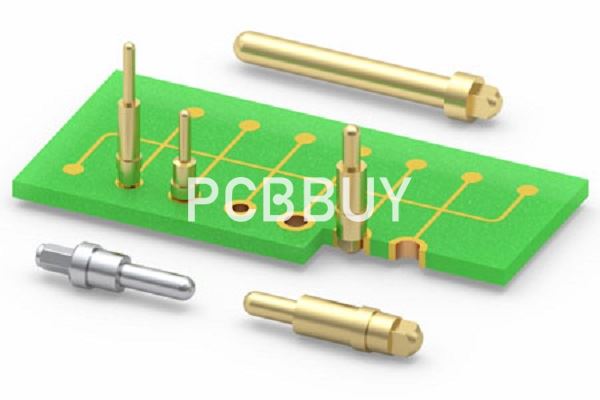
PCB tooling holes, or mounting holes, are circular openings made at the edge of a PCB. Tooling holes are non-plated, and they are used by machines to hold the PCB down for alignment. During the fabrication process. If you’ve ever visited a PCB production facility, you’ll find that it’s filled with machines for the entire manufacturing flow. These machines turn a PCB manufacturing file into a physical PCB, and later, populate it with components. Precision is key to ensure that the final product is free from issues—PCB tooling holes design plays an important role in this.
How to determine the right size for tooling hole in PCB?
Usually, common sizes like 1mm, 1.5mm, and 2mm are acceptable tooling hole sizes for most manufacturers. If you’re unsure, make sure to consult with your PCB manufacturer. For uniformity, you’ll want to stick with a common size for all tooling holes on a PCB.
Besides size, you’ll also need to ensure that the PCB tooling hole isn’t plated. A non-plated hole is better in terms of accuracy compared to a plated one. Also, ensure that there is a solder mask expansion that slightly extends over the hole.
What are the features of tooling Hole in PCB?
If you’ve ever visited a PCB production facility, you’ll find that it’s filled with machines for the entire manufacturing flow. These machines turn a PCB manufacturing file into a physical PCB, and later, populate it with components. Precision is key to ensure that the final product is free from issues—PCB tooling holes design plays an important role in this.
PCB tooling holes, or mounting holes, are circular openings made at the edge of a PCB. Tooling holes are non-plated, and they are used by machines to hold the PCB down for alignment. During the fabrication process, it’s imperative that the PCB be kept still and properly aligned for drilling. If the PCB is not kept still, it will be impossible to deliver precisely-drilled holes.
When the fabricated PCB is sent for assembly, the tooling holes will be needed again if there are SMD components in the design. The machines will use the tooling holes for stencil alignment when applying solder paste and placing SMD components with the pick-and-place machines.
It is important to note that PCB tooling holes should not be confused with fiducial markers. Fiducial markers are pads that are created on the PCB to provide a reference for optical pick-and-place machines. However, both are equally important when designing a PCB with SMD components.

How to process tooling hole tolerance in PCB?
Once you know your maximum lead size, you can begin to calculate the finished hole size. The primary concern is to make the hole large enough that the component lead can be inserted without any problems. Although a loose and sloppy fit can be difficult to work with and solder, a hole that is too small for the lead can lead to huge problems if you try to enlarge it. You could end up ripping out the metal plating of the hole and or breaking the signal traces connecting to the hole.
Here are some other considerations to remember:
· Aspect ratio: This is the ratio between the thickness of the board and the drill hole diameter. For example, a board that is 62 mils thick with a 10-mil drill will have an aspect ratio of 6:1. Most manufacturers can reliably fabricate a board with up to a 6:1 aspect ratio, and larger ratios will increase the manufacturing cost. This is because the larger the aspect ratio, the more difficult it is to plate the hole. Be careful, therefore, that you don’t specify too small of a hole that will force a larger aspect ratio.
· Drill tolerance: Mechanical drills will change subtly with use, and they may vibrate slightly in the hole, causing the hole to be a little oversized. Therefore, drill sizes are assigned a tolerance to account for that. Manufacturers usually prefer plus or minus 3 to 4 mils, but smaller tolerances can be specified for additional costs.
· Plating: To conduct electrical signals through the hole, it will be plated with metal. The depth of the plating will vary depending on the board type and materials, but you should expect the hole size to decrease by 3 or 4 mils after plating.
· To sum it up, your finished hole size should be:
Lead size + the tolerance for the maximum lead size + the drill tolerance and the extra size before plating.
The values will all vary slightly depending on the manufacturer that you use, and you should get their specified tolerances for accuracy. In general, though, a 7-mil-over-the-lead-size rule of thumb is often used by designers for determining a finished hole size.
Industry Category


