What Is Pcb Wiring Strategy
By: 03/20/2024 10:57

Layout is one of the most fundamental skills for PCB design engineers. The quality of routing directly impacts the performance of the entire system, and most high-speed design theories ultimately need to be implemented and verified through Layout. Therefore, routing is crucial in high-speed PCB design. Below, we will analyze the rationality of some situations that may be encountered in actual routing and provide some optimized routing strategies, focusing mainly on right-angle routing, differential routing, and serpentine routing.
Right-angle routing
Right-angle routing is generally something to be avoided in PCB routing and has become one of the standards for measuring routing quality. But how much does right-angle routing affect signal transmission? In principle, right-angle routing causes a change in the width of the transmission line, leading to impedance discontinuity. In fact, not only right-angle routing but also acute and obtuse angle routing can cause impedance variation.
The effects of right-angle routing on signals mainly manifest in three aspects: first, corners can be equivalent to capacitive loads on transmission lines, slowing down the rise time; second, impedance discontinuity can cause signal reflection; third, EMI generated by right-angle tips.
If you want to order PCB product, please check and custom your order online.
The parasitic capacitance brought by right-angle routing can be calculated using the empirical formula:
C=61W(Er)1/2/Z0
In this formula,
C
C represents the equivalent capacitance of the corner (unit: pF),
W
W is the width of the trace (unit: inch),
ε
r
ε
r
is the dielectric constant, and
Z
0
Z
0
is the characteristic impedance of the transmission line. For example, for a 4-mil 50-ohm transmission line (
ε
r
ε
r
is 4.3), the capacitance brought by a right angle is approximately 0.0101 pF. This can then be used to estimate the change in rise time caused by this:
Through calculation, it can be seen that the capacitive effect brought by right-angle routing is extremely small.
Due to the increase in trace width caused by right-angle routing, the impedance at that point will decrease, leading to certain signal reflection phenomena. We can calculate the equivalent impedance after the width increase according to the impedance calculation formula mentioned in the transmission line section, and then calculate the reflection coefficient using the empirical formula:
ρ=(Zs-Z0)/(Zs+Z0)
Generally, the impedance variation caused by right-angle routing is between 7% and 20%, so the maximum reflection coefficient is around 0.1. Moreover, from the diagram, it can be seen that the impedance of the transmission line changes to a minimum within the length of
W
/
2
W/2 and then returns to normal impedance after
W
/
2
W/2 time. The entire impedance cha
T10-90%=2.2*C*Z0/2=2.2*0.0101*50/2=0.556ps
nge occurs very quickly, often within 10 ps, so such fast and minute changes can be almost ignored for general signal transmission.
Many people have the understanding that right-angle routing is prone to emit or receive electromagnetic waves, resulting in EMI. However, many actual test results show that right-angle routing does not produce significantly more EMI than straight lines. Perhaps the current instrument performance and testing level limit the accuracy of the tests, but at least it illustrates a point: the radiation of right-angle routing is smaller than the measurement error of the instrument itself. Overall, right-angle routing is not as scary as imagined. At least in applications below GHz, any effects such as capacitance, reflection, EMI, etc., caused by it are hardly reflected in TDR tests. The focus of high-speed PCB design engineers should still be on layout, power/ground design, routing design, vias, and other aspects. Of course, although the impact of right-angle routing is not very serious, it does not mean that we can always use right-angle lines in the future. Paying attention to details is a basic quality that every excellent engineer must possess. Moreover, with the rapid development of digital circuits, the signal frequency handled by PCB engineers will continue to increase. In the RF design field above 10 GHz, these small right angles may become the focus of high-speed problems.
Differential routing
Differential signals are increasingly widely used in high-speed circuit design, and the most critical signals in the circuit often adopt a differential structure. What makes it so popular? And how can its good performance be ensured in PCB design? With these two questions in mind, let's discuss the next part.
What is a differential signal? Simply put, it is when two equal and opposite signals are sent from the driving end, and the receiving end determines the logic state "0" or "1" by comparing the difference between these two voltages. The pair of traces carrying the differential signal is called a differential pair.
Compared with ordinary single-ended signal routing, the most obvious advantages of differential signal routing are manifested in three aspects:
a. Strong anti-interference ability: because the coupling between the two differential traces is very good, when there is external noise interference, it is almost simultaneously coupled to both lines. Since the receiving end only cares about the difference between the two signals, external common-mode noise can be completely canceled out.
b. Effective EMI suppression: Similarly, due to the opposite polarity of the two signals, the electromagnetic fields radiated to the outside by the two signals can cancel each other out. The tighter the coupling, the less electromagnetic energy is leaked to the outside world.
c. Accurate timing: Because the switching of differential signals occurs at the intersection of the two signals, rather than relying on two threshold voltages like ordinary single-ended signals, it is less affected by process and temperature, which can reduce timing errors and is also more suitable for circuits with low amplitude signals. The currently popular LVDS (low voltage differential signaling) refers to this small amplitude differential signal technology.
For PCB engineers, the primary concern remains how to fully leverage the advantages of differential routing in practical routing. Perhaps anyone who has worked with Layout will understand the general requirements of differential routing, which are "equal length, equal spacing." Equal length ensures that the two differential signals always maintain opposite polarities, reducing common-mode components; equal spacing mainly ensures that the differential impedance is consistent, reducing reflections. The "keep it close principle" is sometimes also a requirement for differential routing. However, all these rules are not meant to be applied rigidly, and many engineers seem to misunderstand the nature of high-speed differential signal transmission in PCB design. Below, let's discuss some common misconceptions in PCB differential signal design.
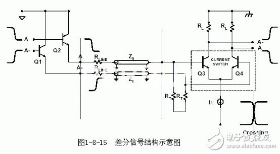
Misconception 1: Believing that differential signals do not need a ground plane as a return path or that differential traces provide each other with return paths. The reason for this misconception is being misled by surface phenomena or not having a deep enough understanding of the mechanism of high-speed signal transmission. From the structure of the receiver in Figure 1-8-15, it can be seen that the emitter currents of transistors Q3 and Q4 are equal in value but opposite in direction. Their currents cancel each other out at the ground connection (I1=0), making the differential circuit insensitive to noise signals such as ground bounce and other noise signals that may exist on the power and ground planes. The partial cancellation of the ground plane's return current does not mean that the differential circuit does not use the reference plane as the signal return path. In fact, in signal return analysis, the mechanism of differential routing is consistent with that of ordinary single-ended routing. That is, high-frequency signals always return along the path with the smallest inductance. The biggest difference is that differential lines have coupling to ground as well as coupling to each other. Whichever coupling is stronger becomes the main return path. The diagram in Figure 1-8-16 shows the magnetic field distribution of single-ended and differential signals.
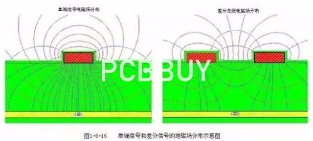
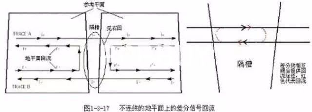
In PCB circuit design, the coupling between differential traces is generally small, often only accounting for 10-20% of the coupling, with the majority being coupling to ground. Therefore, the main return path of differential traces is still on the ground plane. When the ground plane is discontinuous, the coupling between the differential traces will provide the main return path, as shown in Figure 1-8-17. Although the discontinuity of the reference plane has less serious consequences for differential routing than for ordinary single-ended routing, it still degrades the quality of the differential signal and increases EMI and should be avoided as much as possible. Some designers may think that removing the reference plane under the differential traces can suppress some common-mode signals in differential transmission. However, theoretically, this practice is not advisable. How to control the impedance? Not providing a ground impedance return path for common-mode signals will inevitably cause EMI radiation, outweighing the benefits.
Misconception 2: Believing that maintaining equal spacing is more important than matching line lengths. In practical PCB routing, it is often impossible to simultaneously meet the requirements of differential design. Due to factors such as pin distribution, vias, and routing space, line length matching can only be achieved through appropriate routing, but the result is that certain areas of the differential pair cannot be parallel. In such cases, how should we make choices? Before drawing conclusions, let's look at the following simulation results. From the above simulation results, it can be seen that the waveforms of scheme 1 and scheme 2 almost overlap, which means that the influence caused by unequal spacing is negligible. In comparison, the impact of unmatched line lengths on timing is much greater (scheme 3). From a theoretical analysis, although unequal spacing may cause differential impedance to change, because the coupling between differential pairs itself is not significant, the range of impedance change is also small, usually within 10%. It is equivalent to a reflection caused by a via, which does not significantly affect signal transmission. Once the line lengths are unmatched, in addition to timing offsets, common-mode components are introduced into the differential signal, degrading signal quality and increasing EMI.
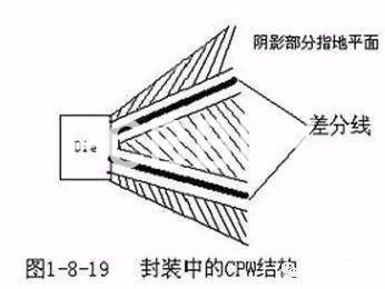
Misconception 3: Believing that differential traces must be placed very close together. Bringing differential traces close together is aimed at enhancing their coupling, which can improve immunity to noise and fully utilize the opposite polarity of magnetic fields to counteract external electromagnetic interference. While this practice is generally advantageous, it's not absolute. If we can ensure that they are sufficiently shielded from external interference, then we don't need to rely on strong coupling to achieve noise immunity and EMI suppression. How can we ensure that the differential traces have good isolation and shielding? Increasing the spacing from other signal traces is one of the basic approaches. The energy of the electromagnetic field decreases with distance squared. Generally, when the spacing between lines exceeds 4 times the line width, the interference between them is extremely weak and can be ignored. Additionally, isolation through the ground plane can provide good shielding. This structure is often used in high-frequency (above 10G) IC packaging PCB designs and is called the CPW (coplanar waveguide) structure, which can ensure strict control of the differential impedance (2Z0), as shown in Figure 1-8-19.
Differential traces can also be routed on different signal layers, but this practice is generally not recommended because differences in impedance, vias, and routing space between layers can degrade differential mode transmission and introduce common-mode noise. Moreover, if the coupling between adjacent layers is not tight enough, it will reduce the ability of differential traces to resist noise. However, if you can maintain an appropriate spacing from surrounding traces, crosstalk is not a problem. At typical frequencies (below GHz), EMI is not a serious issue. Experiments have shown that the radiation energy attenuation of differential traces spaced 500 mils apart reaches 60 dB at a distance of 3 meters, which is sufficient to meet FCC electromagnetic radiation standards. Therefore, designers don't need to overly worry about insufficient coupling of differential lines causing electromagnetic incompatibility issues.
Serpentine Routing
Serpentine routing is a commonly used routing method in Layout. Its main purpose is to adjust delays to meet system timing design requirements. Designers should first understand that serpentine routing can degrade signal quality and change transmission delays, so it should be avoided as much as possible in routing. However, in practical designs, intentional serpentine routing is often necessary to ensure that signals have sufficient setup time or to reduce timing offsets between signals in the same group.
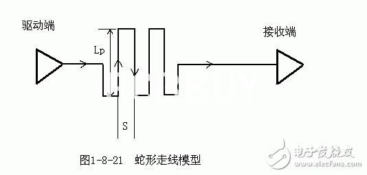
So, what impact does serpentine routing have on signal transmission? What should be noted when routing? The two key parameters are the parallel coupling length (Lp) and the coupling distance (S), as shown in Figure 1-8-21. It is evident that when signals are transmitted along serpentine traces, coupling occurs between parallel segments, appearing in common mode. The smaller the S and the larger the Lp, the greater the degree of coupling. This may lead to reduced transmission delays and significantly degrade signal quality due to crosstalk, as explained in the analysis of common-mode and differential-mode crosstalk in Chapter 3.
Here are some suggestions for Layout engineers when dealing with serpentine routing:
1. Increase the spacing between parallel segments (S), preferably greater than 3H, where H refers to the distance from the signal trace to the reference plane. In simple terms, take wider turns when routing. With a sufficiently large S, mutual coupling effects can be almost completely avoided.
2. Reduce the coupling length Lp. When the delay of twice Lp approaches or exceeds the signal rise time, the crosstalk generated will saturate.
3. Serpentine traces using strip-line or embedded micro-strip structures have smaller signal transmission delays than micro-strip traces. In theory, strip-line traces are not affected by differential-mode crosstalk.
4. For high-speed signals and those with strict timing requirements, try to avoid serpentine routing, especially in small areas.
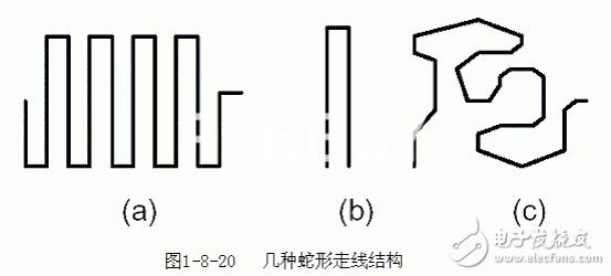
5. Frequent use of serpentine routing with arbitrary angles, such as the C-shaped structure in Figure 1-8-20, can effectively reduce mutual coupling.
6. In high-speed PCB design, serpentine routing does not have filtering or interference resistance capabilities; it can only reduce signal quality and should only be used for timing matching purposes.
7. Sometimes, consider using spiral routing, which simulations have shown to be more effective than normal serpentine routing.
Reprinted from China Electronics Network
Industry Category


