What Is Process of Multilayer PCB Reverse Engineering?
By:PCBBUY 02/23/2024 14:42

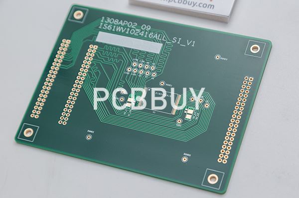
PCB reverse engineering is a multilayered process that includes targeted PCB research, reverse analysis and PCB design technology reproduction. The process is also used to identify and obtain the design of a product’s functional and structural characteristics, as well as the processing flow. With this information, a company can produce products with similar functions and abilities — though businesses will make sure they’re not reproducing an exact replica of a reverse-engineered PCB.
Do you know the basic knowledge of PCB reverse engineering? If you are looking for more information about PCB reverse engineering, please check and read the passage for more professional knowledge.
What is the definition of PCB reverse engineering?
Reverse engineering circuit boards can be a long process, but it’s well worth the payout. There are a few primary stages of reverse engineering PCBs that anyone who attempts to do it should follow. These steps include creating initial drawings, scans or photographs of PCBs that are then uploaded to the appropriate reverse-engineering software and programs. Once uploaded, users have to build the PCB’s layout and use that layout to create schematics.
Reverse engineering is primarily utilized to determine and analyze the design principles behind a product. It’s especially useful when a company can’t easily find design information on a specific product.
The most common method of reverse engineering a PCB involves disassembling a sample PCB and then analyzing it. From this analysis, a company will create documentation about the sample PCB, which various team members can review. This documentation will often include information about how the product is designed and how it operates.
A company can then use the information they gather from a sample PCB to manufacture similar PCBs that may function better than their competitors’ offerings. Alongside reverse engineering’s ability to help companies analyze and outdo competitors’ products, it can also help businesses improve their own PCB offerings. For example, reverse engineering can help them enhance their boards’ functionality by spotting obsolete parts, security issues or poor designs.

What Is Process of Multilayer PCB Reverse Engineering?
· Assign reference designations to unmarked components before starting PCB reverse engineering.
· Create a Component level BOM.
· Design -Identify the system’s components and their interrelationships.
· Components Placement & Mechanical.
· XY locations of Connectors, LED, Switches etc.
· Board mechanical Mounting holes & any special cuts on Boards, Board size etc.
· Download datasheets, application notes, and architecture information.
· Create net list.
· Make the Schematic Drawing and PCB Layout.
Why reverse engineer a PCB?
There are several advantages of reverse engineering PCBs — many companies use these devices for various purposes. Reverse engineering can also help you produce more effective or less costly versions of a competitor’s PCBs.
Learn more about the advantages of reverse engineering PCBs below:
· Maintain crucial PCBs
· Get information on PCBs without documentation
· Reduce your reliance on experts
· Identify weaknesses in a competitor’s designs

What are the considerations of PCB reverse engineering?
Basically figuring out how the PCB works without the original engineering documentation.
You start by creating a schematic by identifying all the components on the board and then finding all of the interconnections. This gives you a schematic which allows you to figure out how the board works. It sound easy but on complex boards in can be extremely time consuming and is frequently made more difficult by the use of complex custom chips. You can actually reverse engineer the actual chips as well, but this is even more specialized and requires a lot of specialized equipment.
One of the common uses for reverse engineering is do determine if competitors are using your patents, hardware or Ontellectual property to make their competing products, but there are other malign reasons. Government security agencies do this kind of thing as well to gain insights into other countries weapons susystems, for example.
There are specialist companies that perform this kind of work for a fee. If you are right and a competitor is illegally using your patents you may get a financial settlement that will cover your costs, but that is not guaranteed.
Industry Category


