What Is SMD in PCB & What Are the Specials of It?
By:PCBBUY 12/31/2021 09:57

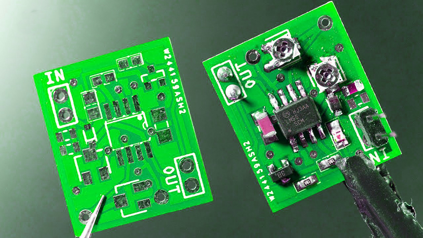
Surface Mounted Devices (SMD) are the parts that are arranged and fixed into a bare board during PCB assembly. We live in the technology age, where consumers demand highly performing, and more flexible, miniaturized, and cost-effective electronic products. SMD serves these purposes well as they have pins that you can solder directly onto boards instead of relying on leads and wires.
Do you know SMD in PCB? If you are looking for the knowledge of SMD in PCB, please check and read the content in this passage below.

Why we choose SMD in PCB?
Dependable Processing
Some manufacturers are using high-performance plastic LCP for making surface mount devices. It makes sure precise grid alignment and maximum dimensional stability. The material has tremendous solder heat resistance. Therefore, a smooth, dependable SMD connection system is guaranteed.
You will not need to pre-dry such SMDs as they have low moisture sensitivity (MSL 1). They also have a low thermal expansion coefficient, which prevents a PCB assembly from being dismantled during soldering. Therefore, you can rapidly perform the whole automatic PCB assembly process.
Stable Solder Connections
The PCB terminals of SMDs made using LSF make sure a firm grip on the board. It is because the manufacturers use two solder pads for each pole. You can even place large electronic components as the holding force/pin is more than 150 N.
Manufacturers also perform endurance tests to make sure the shock resistance and high vibration are according to IEC 61373/10.2011. Thus, you will get a maintenance-free and smooth SMD process in the long run.
Effective Assembly
SMD with suction surfaces support and pick-and-place pads ensure accurate placement and safe mounting in the automatic PCB assembly process. You will also be maximizing the performance of the assembly due to the lightweight of the PCB terminals of SMD.
Coming to the packaging of these components, you will get them in standard conveyor widths with tape-on-reel packing. Furthermore, they are made for automatic processes and thus contain many numbers of features for every roll. What does it mean? It just means that you are reducing your setup expenses.

What are the features of SMD in PCB?
· Dense assembly of the components on the printed circuit board
· Double-sided PCB assembly
· Improved electrical properties of the circuit, particularly at higher frequencies
The higher component density in the SMD assembly allows for greater miniaturisation of circuits and assemblies and thereby helps to reduce costs.
What are the differences of SMD VS SMT?
The SMT uses a mounting technology of mounting and soldering surfaces that will be used on the PCB. On the other hand, the use of the SMD refers to using the electronic component that can be placed on a PBC by using the SMT tools. The technique uses components that are soldered on the PCB using a soldering paste.
When it comes to manufacturing the SMT is one that is mostly used since it is cost-effective. The SMT will also offer stronger bonds, ideal for components that are under stress, and one that is good for prototyping.
What are the types of SMD components?
Obviously, your first decision when selecting components is whether to use a through-hole or SMD. Your choice affects your board fabrication and PCB assembly. However, in most cases, especially where size is a factor, you will most likely have to include some SMDs, which can be grouped according to size or package type. Passive devices are available in a range of package sizes, with 0402 (1.0mm x 0.5mm) being one of the most common. Integrated circuits (ICs), which also may come in different sizes, are typically categorized by package type. A few of the most used standard types are listed below:

· Small Outline Integrated Circuit (SOIC)
· Small Outline Package (SOP)
· Small Outline Transistor (SOT)
· Shrink Small Outline Package (SSOP)
· Thin Small Outline Package (TSOP)
· Thin Shrink Small Outline Package (TSSOP)
· Quarter-size Small Outline Package (QSOP)
· Very Small Outline Package (VSOP)
· Flat Packages (there are many variants for flat packages, but the quad form factor is the most common).
· Quad Flat Pack (QFP)
· Quad Flat No-Lead (QFN)
· Plastic Leaded Chip Carrier (PLCC)
· Ball Grid Array (BGA)
· Chip Scale Package (CSP)
· The SMD packages listed above can be acquired in different sizes; however, the form factor will be consistent. Of those listed, the QFN, BGA and CSP must typically be routed using vias.
Industry Category


