What Is Tenting Vias & What Are the Features in PCB?
By:PCBBUY 02/26/2022 10:17

Vias can be very negligible in size, but they are crucial parts of a printed circuit board (PCB). Vias are used to interconnect the copper traces present on different layers of a multi-layered PCB. You will never find any component lead passing through the hole of a via. There are different types of vias, and drilling holes on the PCB make all of them.
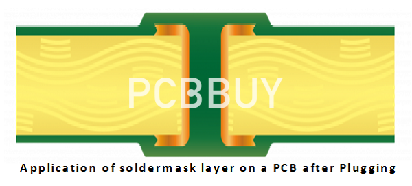
A via may be tented or left exposed — a tenting of a via means that solder mask has been used to cover the via over the hole in the shape of a tent or a skin. Earlier, manufacturers had to face difficulty in tenting the vias as they used liquid photo-imageable (LPI) solder mask. But with the introduction of the dry film solder mask, the process has become much more comfortable.
When to choose tenting vias in PCB?
Whether or not you tent a via comes down to the design of the PCB and the size of the via. Typically, smaller vias are easier to fill or tent. When the via becomes 15mil in diameter, it ends up being too large for the tenting method.
Tenting vias providing extra protection for the hole and copper elements around it. If left exposed, the outside elements can cause the copper to corrode and damage the PCB. With the tenting method being cost-effective as well, the advantages of tenting a via outweigh the disadvantages. For via-in-pad technology, non-conductive via fill should be considered.
What are the advantages and disadvantages of tenting vias in PCB?
Advantages
Tenting vias has many advantages for a PCB, the first being the protection the solder mask provides to the vias. Just like the solder mask prevents the copper traces from oxidizing and corroding, the solder mask does the same thing for the via. Tenting via creates a barrier that can help prevent any damages to the PCB layers.
Using the tenting method also reduces the number of conductive components that are exposed to external elements. When left exposed, the elements can decrease the integrity of the components and lead to corrosion. It also helps reduce the possibility of a short from happening from solder bridging.
Tenting vias are a cost-effective way of providing protection to the vias and the copper around it. Tenting a via with liquid photoimageable solder mask is the most cost-effective way of tenting.
Disadvantages
Tenting vias is not the most effective method for covering the via. One downside to tenting is that since the solder mask used is liquid, there is the chance of the LPI breaking and creating small holes in the tent. That small hole can trap in moisture and chemicals that can cause corrosion and damage the PCB.
When the PCB is in the prototype phase of the manufacturing process, leaving the vias exposed helps to find any issues with the traces, allowing you to fix and reroute them. Covering the vias could limit the opportunity to find these issues and fix them before it’s too late.

How to make the decision to tent via?
Two major aspects go in to decide whether or not you should tent via. The first, of course is the PCB design and the second is the size of via.
As a thumb rule, tenting works well with vias of smaller diameters of 12 mil or less. Any via that is above 12 mil in diameter does not lend itself to tenting. If you need to take care of large vias closing it with some kind of fill is a far better alternative.
Tenting is also preferred on account of its lower cost as opposed to mask plugging or epoxy filling. In fact tenting via with a liquid photo-imageable solder mask turns out to be the most cost-effective. However where there are concerns about tenting being loose, epoxy filling is an alternative, even though it comes at a higher cost.
Why is PCB tenting via important?
PCB tenting vias is a common practice to protect printed circuit boards. It is often preferred over mask plugging or epoxy filling due to cost. Tenting a via with liquid photoimageable solder mask is the most cost-effective method of tenting. If you are concerned about the tenting being loose and exposing the annular ring, you can choose the more expensive resin filling.

The main goal of tenting via is to leave fewer conductive pads that are exposed on the surface of the board. Conversely, it means that there are fewer shorts during solder bridging in assembly. What’s more, tenting via also can reduce the paste migration from SMT pads, which will take place while drilling the vias on standard BGA “dog-bone”patterns or while the vias are on the edges of SMT pads. As well as tenting vias can make sure that the via won’t be damaged by exposure to the elements.
In general, tenting is more effective with small vias (diameter of 12 mil or less), so you need to consider closing the via instead with some kind of fill if you have larger vias that you need to protect. Obviously, it will not make an effect on conductivity with filling the vias because electrical travel through the copper plating is unimpeded.
Industry Category


