What Is Via Stitching and What Is the Function?
By:PCBBUY 04/20/2022 09:55

Stitching vias do have some concerns to be aware of though. The first is that the high current traces will also be conducting heat. The stitching vias will absorb this heat, but the heat still needs to be dissipated through a thermal via to an external layer of the board for cooling. The stitching vias don’t have to be large, but there have to be enough of them to conduct all of the current and heat without being overloaded. You also need to ensure that you have provided an adequate current return path in your design. In some cases, multiple traces and stitching vias end up taking the place that was needed for a current return path and create a current loop instead.
Are you going to learn the information of PCB via stitching? If you are curious about the PCB via stitching, please check and read the content in this passage for more professional knowledge.
How to process PCB via stitching?
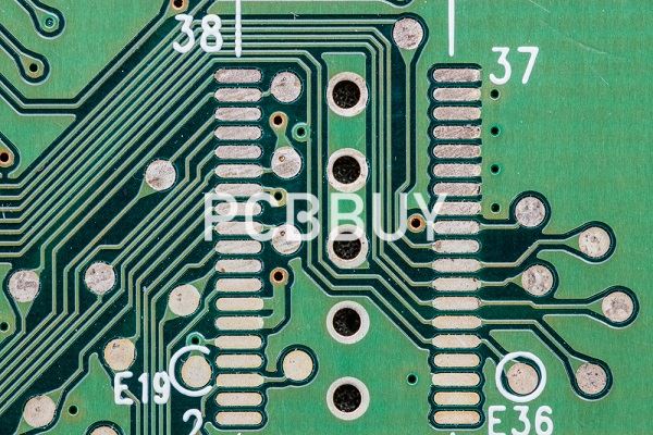
Via stitching is run as post-process, filling free areas of copper with stitching vias. For via stitching to be possible, there must be overlapping regions of copper that are attached to the specified net, on different layers. Supported regions of copper include Fills, Polygons and Power Planes.
Select the Tools to Via Stitching/Shielding to Add Stitching to Net command from the menus to add stitching vias to a specific net. The Add Stitching to Net dialog will open, where the Stitching Parameters and Via Style are specified. Using the selected net, the stitching algorithm identifies all Fills, Polygons and Power Planes attached to that net and attempts to connect them through the board, using the specified via and stitching pattern.
The via stitching algorithm treats Polygons, Fills and Planes in the following way:
· Polygons and Fills that are on the same net are stitched wherever they overlap on different layers. If there are Polygons or Fills on other nets that are overlapping within that area (on another layer), stitching is not applied in that region. Overlapping Plane regions on other nets are passed through.
· Overlapping Plane regions on the target net are always stitched, regardless of the presence of Plane regions (on another layer) attached to other nets. Rule 1 above applies if there are Polygons or Fills overlapping in the same region.

How to add stitching vias?
Via stitching is run as post-process, filling free areas of copper with stitching vias. For via stitching to be possible, there must be overlapping regions of copper that are attached to the specified net, on different layers. Supported regions of copper include Fills, Polygons and Power Planes.
Select the Tools » Via Stitching/Shielding » Add Stitching to Net command from the menus to add stitching vias to a specific net. The Add Stitching to Net dialog will open, where the Stitching Parameters and Via Style are specified. Using the selected net, the stitching algorithm identifies all Fills, Polygons and Power Planes attached to that net and attempts to connect them through the board, using the specified via and stitching pattern.
The via stitching algorithm treats Polygons, Fills and Planes in the following way:
· Polygons and Fills that are on the same net are stitched wherever they overlap on different layers. If there are Polygons or Fills on other nets that are overlapping within that area (on another layer), stitching is not applied in that region. Overlapping Plane regions on other nets are passed through.
· Overlapping Plane regions on the target net are always stitched, regardless of the presence of Plane regions (on another layer) attached to other nets. Rule 1 above applies if there are Polygons or Fills overlapping in the same region.
· Configuring the Stitching Parameters
· Notes about the Add Stitching to Net dialog settings:
Select the Net to be used for stitching first as this effects the behavior of other options, such as clicking the Load values from Routing Via Style Rule button. The Net dropdown is toward the bottom of the dialog, in the middle.

The Grid is the distance between the centers of adjacent stitching vias and applies in the X and Y directions. Stitching vias will not be placed in violation of applicable design rules if a potential via site would result in a violation, that site is skipped.If the Stagger alternate rows option is enabled, alternate rows of stitching vias are offset by half of the Grid value.
The Same Net Clearance options control the clearance between stitching vias and vias and pads on the same net. There are two ways of controlling the clearance between same-net objects, either the applicable Clearance design rule is used, or the Default Via/Pad Clearance specified in the dialog is used. If an applicable rule exists, then the tighter of these two settings is used. Use the Create new clearance rule button to add a new Clearance design rule into the rules dialog, based on the settings you have entered in the Default Via/Pad Clearance field.
The stitching Via Style can be configured manually, or it can be selected from those available in the Template dropdown, or it can be imported from the applicable Routing Via Style design rule by clicking the Load values from Routing Via Style Rule button. Clicking this button will load the Preferred rule settings.
Industry Category


