What Is Yogurt Machine Pcb?
By: 09/11/2023 10:34
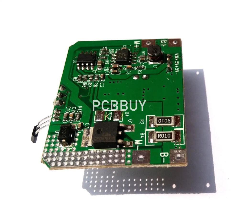
A yogurt maker is a household appliance used for producing yogurt. With increasing consumer interest in healthy eating and advancements in food processing technology, the market demand for yogurt makers is growing. As a critical component of yogurt makers, the design and manufacturing of PCBs (Printed Circuit Boards) have a crucial impact on the performance and lifespan of these machines.
what is a yogurt machine?
A yogurt maker is a machine designed for producing yogurt by providing a constant temperature environment for milk fermentation, typically within the range of 35-45 degrees Celsius. In this setting, probiotics proliferate, and lactose in the milk is converted into lactic acid, resulting in the fermentation of milk into yogurt.
Basic Concepts and Characteristics of PCB
A printed circuit board (PCB) is a substrate or board used to interconnect electronic components and features circuit patterns and traces. PCBs possess the following characteristics:
l Facilitates high-density and high-reliability connections.
l Suitable for mass production, reducing manufacturing costs.
l Can meet various special requirements, such as high-temperature resistance, moisture resistance, and dust resistance.
l Allows for automated production, improving manufacturing efficiency.
To place an online order for yogurt maker PCB, please click here.
PCB Manufacturing Process and Workflow
PCB manufacturing primarily involves the following processes and workflow:
Mask Making: Based on the designed circuit patterns and traces, mask templates are created for forming circuit patterns and traces on the PCB.
Substrate Treatment: The PCB substrate undergoes treatment processes such as cleaning and drying to ensure flatness and cleanliness.
Coating: A layer of conductive material, such as copper or nickel, is coated onto the substrate to create circuit patterns and traces.
Exposure: The prepared mask templates are placed on the coated substrate and exposed using an exposure machine to form circuit patterns and traces.
Etching: The exposed substrate is immersed in etching solution to dissolve unwanted copper, leaving behind the desired circuit patterns and traces.
Surface Treatment: The surface of the circuit patterns and traces is treated, such as with oxidation resistance or gold plating, to enhance conductivity and corrosion resistance.
Inspection and Testing: The manufactured PCBs undergo inspection and testing to ensure they meet design specifications and quality standards.
Yogurt Maker PCB Design Process
The PCB design process for a yogurt maker includes the following steps:
Define Design Specifications: Based on the yogurt maker's design requirements and functionality, determine the circuit schematic and overall design plan.
Component Selection: According to the design plan, determine the type, specifications, and parameters of the required electronic components.
Component Layout: Arrange the selected components on the PCB according to the circuit schematic and wiring requirements.
Signal Integrity Analysis: Analyze PCB signal integrity based on the circuit schematic and component performance parameters, optimizing signal quality and transmission performance.
Electromagnetic Compatibility Analysis: Evaluate PCB electromagnetic compatibility according to the yogurt maker's electromagnetic environment and usage requirements, optimizing electromagnetic performance and interference suppression capabilities.
Generate Production Files: Convert the designed PCB files into production files, including Gerber files, drill files, etc., for PCB manufacturing.
Review and Testing: Conduct functional tests, signal tests, electromagnetic compatibility tests, and other checks on the manufactured PCB to ensure it meets the yogurt maker's performance and usage requirements.
Yogurt Maker PCB Design Process
2.1 Circuit Design
In the PCB design of a yogurt maker, circuit design is the most fundamental and critical step. The quality of circuit design directly impacts the performance and stability of the yogurt maker. During circuit design, factors such as the operational principles, performance specifications, and application environment of the yogurt maker need to be taken into consideration. Rational circuit designs are developed based on these factors.
2.2 Component Layout
After completing the circuit design, the next step is component layout. Component layout is a crucial phase in PCB design, as it directly affects the performance and reliability of the yogurt maker. When performing component layout, factors such as the interaction between components, heat dissipation, and maintainability need to be considered. Component positions and orientations are arranged sensibly based on these factors.
2.3 Signal Integrity Analysis
Following component layout, a signal integrity analysis is necessary. Signal integrity analysis aims to ensure that signals do not experience errors or distortion during transmission. During signal integrity analysis, factors such as signal amplitude, frequency, transmission delay, etc., are taken into account. Circuit optimization and adjustments are made based on these factors.
Manufacturing Process and Workflow for Yogurt Maker PCB
3.1 Manufacturing Process
The manufacturing process for a yogurt maker PCB primarily includes the following steps:
Frame Production: Select appropriate materials and create frames according to design requirements. The size and shape of the frame should be designed to meet practical needs.
Circuit Fabrication: Transfer the pre-designed circuit patterns onto the frame using methods like chemical etching or laser engraving.
Hole Drilling: Create necessary holes on the frame to allow for component insertion and soldering.
Application of Solder Mask: Apply a solder mask layer on the board's surface during the soldering process to prevent direct contact between components and the board, preventing short circuits.
Component Soldering: Solder all components onto the frame and conduct inspections to ensure the circuit's proper functionality.
Testing and Inspection: After all soldering is completed, conduct functional testing and inspections to ensure product quality meets the required standards.
3.2 Manufacturing Workflow
The manufacturing workflow for a yogurt maker PCB mainly involves the following steps:
Incoming Material Inspection: Inspect all raw materials to ensure they meet production requirements.
Pre-processing: Clean the frame's surface thoroughly to facilitate subsequent operations.
Hole Drilling: Create the necessary holes on the frame.
Application of Solder Mask: Apply a solder mask layer on the board's surface to prevent short circuits during soldering.
Solder Paste Printing: Print solder paste onto the board at the designated locations for component soldering.
Component Placement and Fixation: Place all components onto the board and secure them in place.
Soldering: Use high temperatures to solder components to the board's circuits.
Visual Inspection: Perform a visual inspection of the completed circuit board to identify any soldering defects or discrepancies. If any defects are found, perform necessary rework to ensure product quality and reliability.
Testing and Inspection: After all soldering processes are completed, conduct functional testing and inspections. Only PCBs that pass these checks proceed to the next stage.
Electrical Performance Testing: Confirm the continuity and insulation of all conductive lines on each PCB through comprehensive testing using specialized equipment. If any anomalies are detected, return the PCB for repairs.
Industry Category


