What Is copper surface treatment for PCB ?
By:PCBBUY 12/24/2024 16:27
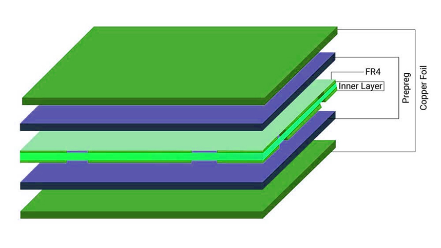
Multilayer PCB is one of the important types of PCB, using the subtraction method, multiple single-layer laminated composite manufacturing technology is still the mainstream manufacturing technology of multilayer PCB. New requirements for copper surface treatment technology before lamination of multi-layer PCB after multi-layer structure of PCB and high-speed and high-frequency signal transmission are proposed, as well as technical methods formed to meet these requirements, including: Basic principles and technical characteristics of copper surface treatment, copper surface mechanical treatment technology, brown technology, bleaching technology, and copper foil surface treatment effect evaluation method.
Overview of copper surface treatment for PCB
Overview of pretreatment technology of copper surface before lamination
What Are the Meaning and Purpose?
In the era of single-panel and low-frequency communication, the effect of the roughness of the electronic circuit on the electrical performance of the whole machine can be ignored. With the high-speed and high-frequency signal transmission in electronic equipment, the surface properties (such as roughness) of the electronic circuit and the carrier substrate become very important and become an important part of determining the integrity of the system signal. In addition, the multi-layer thinning of the PCB is an important way to improve the density, and the requirements of interlayer bonding force and ion mobility resistance reflect the importance of pretreatment of the copper foil surface before laminating.
In the manufacturing process of multi-layer PCB, improving the interlayer bonding force and controlling the surface roughness of the conductor are always the key points to improve the quality of the PCB product. The copper surface treatment technology before lamination of PCB refers to the technology that uses physical and chemical means to modify the copper foil and resin on the surface of the substrate by limited etching or adding coating, changing the surface characteristics such as the roughness and chemical affinity of the copper foil and the insulating substrate to achieve the goal of improving the binding force of the multi-layer board and the electrical performance of the PCB (such as improving the integrity of high frequency signals). Such as blackening technology, micro-etching technology, brown technology and so on. Improving the bonding force between layers of multilayer plates can effectively prevent the phenomenon of "exploding board" and "whitening", and controlling the roughness can effectively improve the quality of signal transmission. The surface treatment technology of printed lamination includes resin matrix surface treatment and copper foil matrix surface treatment. This paper mainly introduces the surface treatment technology of copper foil.
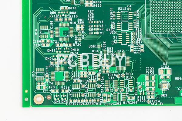
Multi-layer boards can achieve higher packaging density, skin effect of high frequency signals
When there is an alternating current or alternating electromagnetic field in the conductor, the current inside the conductor is not evenly distributed, and the current is concentrated in the "skin" part of the conductor, that is, the current is concentrated in the thin layer on the surface of the conductor, the closer to the surface of the conductor, the greater the current density, and the actual current inside the conductor is smaller. As a result, the resistance of the conductor increases, so does its loss power. This phenomenon is called the skin effect.
Determines the importance of the surface properties of copper foil, and also lays the important position of its surface treatment technology. Therefore, the substrate surface treatment technology has become a research hotspot in PCB manufacturing, foreign countries have long begun to carry out a lot of research on the surface treatment process of copper foil, while domestic research on the surface treatment process of copper foil started late, and related products lack market competitiveness.
Technical classification of copper surface treatment
Tracing the production process of multi-layer PCBs can be seen that the upper and lower surfaces of the transmission line in the PCB correspond to the smooth surface and rough surface of the copper foil of the copper-covered plate. Since the copper foil surface has been pressed on the glass fiber cloth of the copper clad plate, its surface state will not change, and the roughness of the copper foil surface is only subject to the type of copper foil. The smooth surface of copper foil will be subjected to a series of physical and chemical treatments in the processing process, which may change the surface state, so the roughness of the rough surface of copper foil is jointly affected by the type of copper foil and the roughening process. Copper foil type is the determining factor of surface roughness under the transmission line, and copper foil type and roughening process are the common influencing factors of surface roughness on the transmission line.
PCB substrate (copper foil, resin substrate) surface adhesion enhancement technology belongs to the category of surface treatment technology, according to its principle of action can be divided into two categories: physical method and chemical method. According to the different materials and means used, it is divided into mechanical brushing technology, plasma etching technology, blackening technology, brown technology and many other types.

The classification overview is as follows:
Physical method:
(1) Mechanical brushing technology: simple process, low cost, large surface roughness value after treatment, easy to lead to deformation of the inner plate. Not applicable to high frequency board field.
(2) Volcanic ash brush technology: simple process, low cost, surface roughness after treatment is less than mechanical brushing technology, easy to lead to deformation of the inner plate.
(3) Plasma etching technology: simple process, high efficiency on organic matter. It is used in micropore cleaning, polymer substrate surface activation and cleaning processes.
Chemical method:
(1) Chemical micro-etching technology: there are many types and large differences between different processes, the process is mature, the use of large surface, the stability of the system is poor, the etching rate is unstable, the uniformity is difficult to control, and there are waste liquid treatment problems.
(2) Blackening technology: Improving the interlayer bonding force is very effective. High cost, long process flow, complex production process, difficult sewage treatment, there are "pink circle" and ion migration problems.
(3) Browning technology: more simple and easy to control than the blackening technology process, good acid resistance of the Browning film, the brown layer does not produce pink rings, the binding force is not as good as the blackening technology, and the challenges in the field of lead-free welding
(4) Can take into account the dual requirements of improving interlayer bonding force and reducing coarsening degree, and the current process maturity is poor, which belongs to a new generation of technology
Other methods:
Sputtering technology, ion implantation technology:
Simple process, high equipment investment, high cost, limited to special requirements.
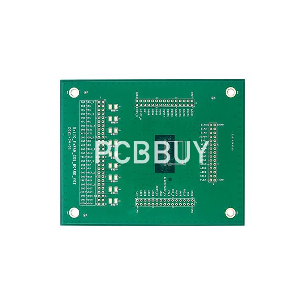
Pink circle:
After the surface of the plate is oxidized, a villous layer (copper oxide and cuprous oxide) is formed. In essence, the villi will be dissolved by acid or reducing solution, making the original black or reddish-brown villi a red copper color;
After the plate is pressed and drilled, the copper color ring with obvious dissolution color contrast appears in the pile around the hole, which is called pink ring.
In the multi-layer PCB manufacturing process, the pink bare copper surface produced after the inner layer copper foil surface oxide is dissolved is usually said to be the "pink circle".
Comparison of treatment results between blackening technology and Browning technology
(1) Oxidation layer crystallization:
Blackening technology: the blackening oxide film is thicker, the crystallization is longer, the coverage is stronger than the brown film, and the crystal is pinnate
Browning technology: The Browning film is a fine crystalline structure, which has a strong bonding force for lamination
(2) Adhesion strength:
Black: The direct tear strength after laminating is generally maintained above 4.5lb/in
Brown: The tear strength after laminating is generally maintained above 6.0lb/in
(3) Anti-pink ring performance:
Black: The length of the dark pile is not easy to control. If the pile is too short, the surface area of the board is small and the bonding strength is poor. When the villi is too long, the lamination can easily cause the easily broken oxide film to be attacked by the potion and become pink circles
Brown: Through the organic additives in the brown liquid and the organic metal complex generated on the surface of copper, enhance the inner layer and resin bonding force and the thermal shock ability of lamination, strong acid resistance and not easy to produce pink circle.
(4) Electrical problems
Black: Long needle crystals are easy to break and diffuse into the plate with the fluid glue, forming electrical problems
Brown: No electrical problems, but poor heat shock resistance
(5) Color:
Black: the color of the board is easier to control, and the color difference is smaller
Brown: the color of the board is difficult to control, and it is easy to have a large color difference
Basic principles of copper surface treatment technology before lamination:
Classification and characteristics of copper foil
The advancement of electronic products in the direction of intelligence and networking has promoted the PCB to high-frequency and high-speed, high-density, and also put forward more stringent requirements for the performance and quality of the special material for its manufacture - electrolytic copper foil. The use of low profile/ultra-low profile has become one of the effective ways to solve the transmission loss of the high-frequency substrate, and the low roughness copper foil technology has become an important application direction of the PCB industry.
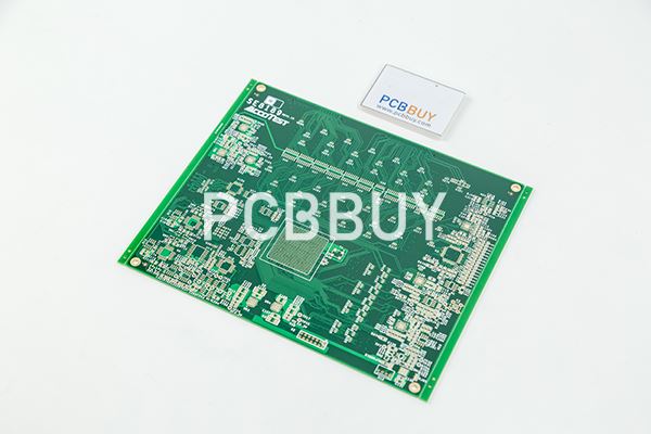
HTE copper foil: traditional electrolytic copper foil;
RFT copper foil: electrolyzed copper foil raw foil is made and the smooth and rough surface of the raw foil are reversed for treatment of copper foil
VLP copper foil, HVLP copper foil: Copper foil with low and ultra-low surface profile after a series of treatments after the raw foil is made
FP copper foil: The surface profile almost approaches the flat state
Principle and process of electrolytic copper foil surface pretreatment
Whether it is electrolytic copper foil or rolled copper foil, the surface treatment should be easy to obtain better performance when used. The conventional electrolytic copper foil surface treatment process is: degreasing -- "washing --" pickling -- "washing --" coarsening -- "curing --" plating barrier layer --"
-- "Surface passivation treatment --" drying
(1) Pretreatment: Clean the surface of raw foil, remove oxides, remove oil and other treatment processes.
(2) Washing: used to remove all kinds of incidental impurities on the surface, the chemical reagents of the previous adsorption treatment, etc
(3) Coarsing and curing treatment: If the pre-treated copper foil is pressed directly with the insulating resin substrate, the bonding strength between the copper foil and the resin substrate is not high, and it is easy to fall off. In order to enhance the binding force of copper foil and resin substrate, it is necessary to rough and cure the surface of copper foil and resin substrate
(4) Plating barrier layer: copper foil plating barrier layer refers to the technology of further coating another layer of metal layer on the copper foil after coarsening and curing. The new coating is located on the copper foil curing layer, and its function is:
* (1) The bonding strength of the treated copper foil on the insulating resin substrate meets the technical requirements of the press plate
* (2) Meet the actual needs of PCB manufacturing in terms of corrosion resistance and ion migration resistance
* (3) Prevent the PCB copper foil from producing rust and spots in the manufacturing process, circuit board short circuit and other phenomena.
* (4) To overcome the shortcomings of easy oxidation and discoloration in the production process of PCBs
* (5) Improve product heat resistance and high temperature corrosion resistance
Electrolytic copper foil can improve the bonding strength between copper foil and substrate through the surface treatment of electroplating barrier layer, and improve the side corrosion resistance, ion migration resistance, heat resistance, acid resistance, corrosion resistance and oxidation resistance of copper foil.
(5) Surface passivation treatment:
In the operation of transportation and storage, the copper foil treated by coarsening, curing, and plating barrier layer often has discolored spots on the surface of the copper foil due to the pollution of external water vapor, dust, oxidants, and handprints. High temperature treatment, copper foil surface will also produce local discoloration. It will affect the weldability of the copper surface, the affinity with the ink, the adhesion, and the line resistance will increase, so the surface of the copper foil must be treated with oxidation resistance. The most common anti-oxidation treatment is passivation method, that is, the copper foil is passivated with chromate solution after reading the barrier layer, so that the copper chromium surface forms a film layer with chromium as the main body. It will not oxidize and discolor due to direct contact with the air, improve the heat resistance of copper foil, ensure the weldability of copper foil and the affinity of ink.
Surface treatment of rolled copper foil
Rolled copper foil is produced by heat treatment after mechanical extrusion. The thinner the rolled copper foil, the higher the manufacturing difficulty, the technical difficulty and the added value of the product are also higher and higher. Calendered copper foil surface roughness is small, more uniform, crystal structure and electrolytic copper foil is different, has better folding resistance and deflection performance than electrolytic copper foil, good performance in signal transmission, mainly used in the manufacture of flexible PCBs and high-frequency circuits, is used in military, aerospace and automotive electronics and other products. With the development of electronic products to the direction of high speed and high frequency, the use of rolled copper foil in civil electronic products is also increasing.
The calendered copper foil is generally treated with a slight coarsing, then blackened (the barrier layer is copper-cobalt-nickel alloy or copper-nickel alloy) or reddened, and the surface treatment is anti-oxidation. Blackened calendered copper foils can be used in the manufacture of microflexible PCBs.
Copper foil treatment on the inner surface
In the production of multilayer PCBs, it is always an important technical means to improve the thermal stability of multilayer PCBs. The good bonding between the copper foil and the substrate in the inner PCB mainly depends on two factors: first, the coarsing degree of the copper foil surface and the coarsing structure and structural characteristics; Second: the adaptability of the coarsening layer on the surface of copper foil to the substrate used.
Copper foil should be corroded before oxidation to make it have a certain roughness, which is achieved through two technologies: first, etching coarser technology, such as the original mechanical brushing, blackening, oxidation methods, etc., forms a very rough appearance on the surface, but its structure is fragile and the bonding strength with the substrate is not high; The second is to improve micro-etching methods, such as bleaching technology and ion implantation technology. The characteristics of the improved technology are that not only the copper foil surface is micro-corroded, but also a new layer of characteristic coating can be generated to control the micro-rough structure of the copper foil surface, so as to achieve the dual goals of improving the bond strength and improving the integrity of signal transmission.
Physical copper surface treatment technology of PCB before lamination
It is the earliest pretreatment technology of copper surface before lamination. According to the process characteristics and the different materials used, it can be divided into mechanical brushing, volcanic ash brushing and plasma etching.
Mechanical brushing technology
Mechanical brushing technology is to use abrasive nylon brush rollers such as emery to brush the moving conductor surface under a certain mechanical pressure to remove the surface oxide layer and pollutants, and finally obtain a clean copper surface with a certain roughness. Due to the large hardness difference between the mechanical abrasive and copper, it will cause a depression in the copper surface and form a defect. Therefore, only when the signal transmission frequency is below 10MHz, the PCB surface treatment can use mechanical brushing technology.
Volcanic ash brush technology
Volcanic ash brush technology refers to the use of nylon brush rollers containing volcanic ash or Al2O3 powder and other abrasive materials to brush the copper foil surface in motion under certain mechanical pressure and humidity to remove the surface oxide layer and pollutants, and finally get clean and have a certain roughness of the copper surface. The hardness difference between volcanic ash and copper is small under wet conditions, so the surface roughness obtained by this method is irregular depression, with a size between 1 and 3um, which can meet the needs of high-frequency signal transmission line, and is currently widely used. However, with the increase of signal transmission frequency, this method can no longer meet the technical requirements, and the chemical coarsening method has become the technical progress direction of the industry.
Plasma etching technology
Plasma is a partially ionized gas, belonging to the fourth form of matter. According to the different excitation frequency, it can be divided into ultrasonic plasma, radio frequency plasma and microwave plasma. The plasma used in the PCB is generally a mixture of CF4 and O2 excited at 13.56MHz to form a radio frequency plasma. It consists of electrons, ions, free radicals, photons, and other neutral particles. Due to the existence of active particles such as electrons, ions and free radicals in the plasma, it is easy to react with the solid surface, and the neutral particles can be a good bombardment of the coarse particle surface. Therefore, the solid surface treated by plasma is not only clean without foreign bodies, but also can change the surface microstructure, which is mainly characterized by uniform etching, so as to achieve the ideal etching degree.
Reference
He Wei, PCB Basic Electrical Information Science and Technology, China Machine Press,146-150
Industry Category


