What Is the Comprehensive Guide of Drill Holes and Hole Metallization of PCB?
By:PCBBUY 04/16/2024 16:50

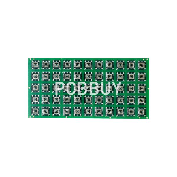
With the rapid development of the electronics industry, the printed circuit board has become more and more demanding for the development of multi-layer PCB and high-density hole lines. A fast circuit board often has thousands or even tens of thousands of holes, so the size of the aperture is also crucial for the density of the printed circuit board. The gradual reduction of pore size makes pore metallization technology more and more important. Only when this step is well controlled can the requirements of multi-layer, high density and small aperture be achieved and quality is guaranteed. Hole metallization is one of the most important processes in printed circuit board manufacturing technology. It is related to the internal quality of the multi-layer printed circuit board, its main work is to drill out the required holes on the multi-layer printed circuit board, remove the drilling dirt in the holes.
What is PCB Drilling and Hole Metallization in PCB?
The development level of rigid printing electrical super theory is generally represented by the value reported in the printing ratio. According to the information, the maximum number of PCB layers has reached 100 layers, and has made 86 layers of the product PCB, capacitors and inductors have the role of tracing the holes on the printed circuit board, one is to supply components such as resistance, and the other is as part of the gas transmission. For 5, the hole is produced in the fine paper printed circuit board and multi-layer printed circuit board, without it, many dense lines and the lines between the middle layer and the layer of the multi-layer printed circuit board cannot be conducted. In order to realize the electrical connection between the layers, the printed circuit board must be perforated metalized, that is, the printed circuit in the two or father house is used for polishing the required baby through the hole, and then a layer of metal is board on the hole wall that can be insulated by chemical coating and electron microscopy.
One of the holes is the core of the two-layered circuit board or multi-layer printed circuit board manufacturing. The requirements of gold absorption holes are very strict, requiring it to have good mechanical toughness and electrical conductivity, while the metallization layer should be uniform, defined between 15-20, in addition, the hole layer is not allowed to have serious oxidation, the hole direction is not stratified, especially bubbles, no drilling chips, especially cracks, the hole resistance is 1000 μm. The following. The quality of deep hole metallization is controlled by three processes: drilling technology, decontamination technology and electroless copper plating technology.
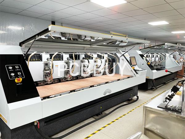
Drilling machine is the use of a variety of drilling machine on the printed circuit board to make different density, different diameter of the through hole. Due to the large number of adhesives such as cyclic vitriol transfer or propanoic acid resin used in the multi-layer printed circuit board substrate, these adhesives, together with copper boxes, polyku and other broken screens, form a sticky dirt on the hole wall under the action of high temperature generated by drilling. If the greasy dirt is not removed, it is easy to cause poor copper plating, resulting in open circuit. Decontamination process is the use of a variety of chemical or physical methods to remove the hole wall dirt, the formation of a clean, with certain characteristics of the hole wall surface, to prevent the failure of the copper plating process, so that the hole wall is not conductive.
In order to form a conductive copper layer in the hole, it is necessary to deposit a thin copper layer several microns thick on the hole wall by a chemical method (ion super exchange method) to lay a conductive foundation for electroplating additive, and then thictify the hole with bright acidic mirror copper solution to achieve the required thickness, and finally realize the metallization of the hole. The individual processes are described in detail below,
What Are the Different Types of PCB Drilling Technique?
The processing methods of printed circuit board through holes include CNC drilling, mechanical punching, plasma etching, laser drilling, and chemical etching and so on. At present, the most widely used are digital drilling and laser drilling, and chemical etching holes have also made great breakthroughs in recent years.
Numerical Control Drilling
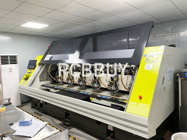
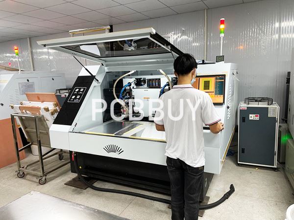
drilling is under the control of the computer using different diameters of the drill in accordance with the corresponding process parameters (speed, feed speed, return speed) on the printed circuit board to get the required through holes. Using a small drill bit, CNC drilling machines can produce microholes with apertures greater than 100um. Although the CNC drilling machine can make microholes with a diameter of less than 100μm on the substrate, the number of layers must be reduced, the drilling speed must be slowed down, and with the drilling diameter becoming smaller, the production efficiency decreases, the production cost increases, the advantage of mechanical drilling is that it can drill holes of all materials, when the aperture is less than 250um, the cost of drilling is increasing exponentially. When the pore size is less than 50μm, the production cost is quite high, the process is difficult, and it is not suitable for large-scale micropore production. The six main factors affecting drilling are drilling machine, drill bit, process parameters, cover board and backing board, processing board and processing environment.
1. CNC Drilling Machine
CNC drilling machines require high stability, high reliability, high speed and high viscosity in order to handle modern printed circuit boards the need for production. CNC drilling machine development has the following characteristics and trends, as a platform.
1) In order to make it rigid and stable enough to avoid small vibration, it is generally used as a large stone or body iron
2) The X-axis and Y-axis substack workbench develops to the X-axis and Y-axis separation workbench, making its weight light, speed improved, increased stability.
3) The multi-spindle drilling machine is gradually driven by each 2 axes separately, that is, one motor drives one shaft.
4) In order to increase speed and accuracy, X axis and Y axis are driven by ball screw DC servo motor to X axis and Y axis ball screw AC servo motor, driving speed up to 50ms.
5) The position accuracy measurement and feedback system is developed from magnetic ruler to grating ruler, and its resolution is high and stable.
6) The X-axis and Y-axis guidance gradually has the trend of replacing the air float guide by the rolling guide, and the rolling guide has good stability and rigidity.
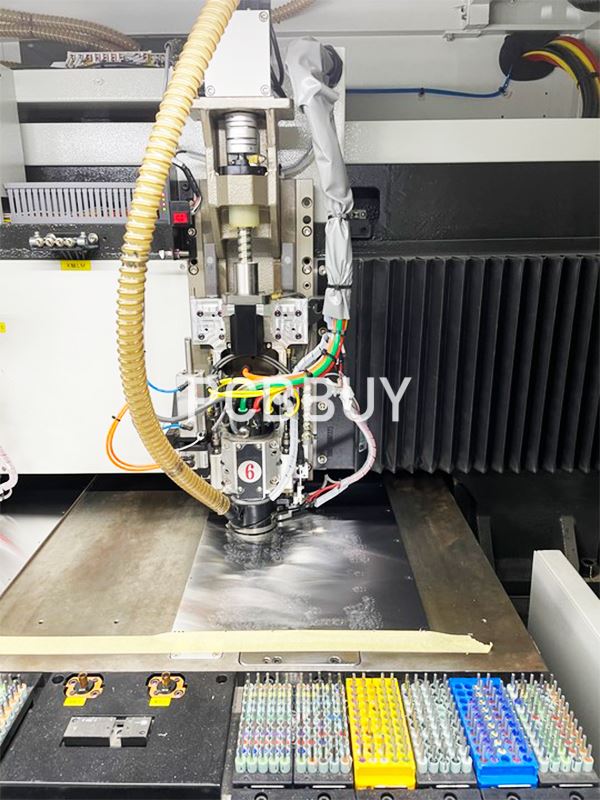
7) Drilling machine spindle is gradually using air bearing high speed spindle.
8) Tool management system includes automatic bit change device (some up to 600 bits), automatic detection system of broken bit, laser detection system (can detect bit diameter, length and radial runout).
9) One hole, one slot positioning system adopts pneumatic clamping to realize automatic loading, positioning clamping and automatic unloading.
10) Use 14in (lin=25.4mm) wide color display screen, clear vision, easy to make fast and accurate selection.
2. Drill Bit
(1) Materials and development trends of drill bits for printed circuit boards 1 Drill bits for printed circuit boards are usually made of hard alloy. Yes. Tungsten carbide is a kind of tungsten drill alloy, tungsten carbide (WC) powder as the base material, cobalt (Co) as the binder, by pressure sintering. It has high hardness, wear resistance and high strength, but the toughness is poor and very face. In order to improve the performance of cemented carbide, the particle size of the powder can be changed, the ratio of tungsten carbide (WC) and drill (Co) can be adjusted, and the WC and Co of different proportions and different particle sizes can be correctly selected according to different specifications of the drill bit.
(2) Types of drill bits Printed circuit board drilling bits have straight shank twist bit, fixed shank twist bit and shovel bit.
a. Straight shank twist drill bit: mostly used in single-spindle drilling machine, mainly drilling simple board or single-sided printed circuit board, drilling depth up to 10 times the diameter of the drill bit. When the substrate layer is not high, the use of drill sleeve can avoid drilling deviation, but it cannot automatically change the tool, and the depth tolerance control is large.
b. Fixed handle twist drill bit: suitable for multi-axis drilling machine, clamping in the special chuck, can achieve automatic clamping, special chuck diameter and fixed handle diameter is the same, there are three models: medium 2mm, 43mm, and 43.175mm. The fixed shank twist bit has high positioning accuracy and does not require the use of drill sleeves. Its large spiral Angle chip removal speed is fast, suitable for high-speed cutting, in the full length of the chip removal slot, the shape of the drill is tapered, drilling and hole wall friction is small, drilling quality is high.
c. Shovel bit: It is to grind the bit edge on the basis of the fixed handle twist bit, retaining 0.6-1.0mm. The length of the edge, the rest of the bit is ground away. The blade bit can reduce the friction between the edge and the hole wall when drilling, reduce the heat accumulation, and reduce the drilling that will cause drilling dirt and fill the multi-layer core board.
3. Cover Board & Backing Board
Printed circuit board drilling using cover board and teaching is very conducive to improving the quality of printed circuit board, improve the yield, although for the use of this auxiliary material will produce a yes, but on the reason, in fact, it is to reduce the cost.
At present, the product board type used in China is 0.3-0.5mm thick phenolic paper glue board and epoxy glass cloth teeth and aluminum boxes. The use of cover board has the following advantages:
a. To prevent burrs on the surface of the gold tie:
b. To protect the copper clad laminate;
c. Prevent the bit from breaking;
d. Improve the accuracy of hole position.
e. low drilling temperature, reduce greasy pollution.
The board is placed on the bottom layer of the printed circuit board to be needle, and the main use of phenolic cardboard or high-density fiber he maintenance board. The use of the pad has the following advantages.
a. Avoid the drilling temperature rise to produce a lot of drilling pollution;
b. Prevent excessive wear and break of drill bit;
c. Prevent the drill bit from drilling into the drilling machine's workbench surface.
4. Drilling Process Parameters
The drilling process parameters include cutting speed, feed speed, retreat speed and bit life. These parameters should be selected and determined according to the specific situation of CNC drilling machine, drill bit, cover board, board and material to be drilled.
Laser Drilling
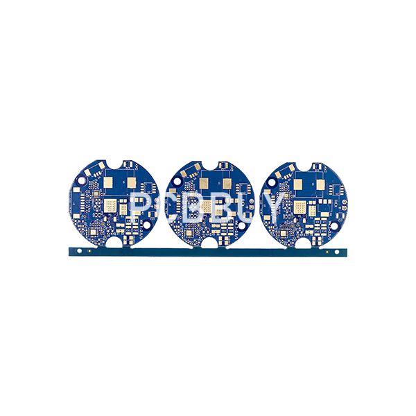
In recent years, with the rapid development of microelectronics technology, mobile phones, computers, digital cameras and other electronic devices are developing to the direction of small, light, high speed and multi-function. The semiconductor devices on these electronic devices are required to be highly integrated and high-speed. Its package from the former flat square closed (QFP) to the miniaturized, multi-pin ball grid array (BGA) or chip level package (CSP) transition. Especially in recent years, the development of high-density interconnect (HDI) printed circuit boards is extremely rapid. The package density requires a small aperture of less than 100μm, a BGA center distance of only 0.8mm, a connection disk diameter of 250um, a solder resistance isolation of only 25μm, and a wire/pitch of less than 50/50μm. The processing of micro-holes is an important step in the production of high-density interconnected printed circuit boards, and laser drilling is the most acceptable processing method for micro-holes at present.
1. The Principle of Laser Hole Formation
Laser is a powerful beam of light excited when the "ray" is stimulated by external stimuli to increase the energy, in which infrared light and visible light have thermal energy, ultraviolet light has optical energy. When this type of light is emitted to the surface of the workpiece, three phenomena occur, namely reflection, absorption and penetration.
The main principle of laser drilling is to remove the processed copper substrate material by means of rotary photo thermal burning and photochemical cracking.
Photo thermal ablation
Photo thermal ablation means that the processed material absorbs high energy laser light and is heated to the surface in a very short time the process by which pores are formed by initiation and natural extension. In this process, the substrate material is subjected to high energy, and there is burned carbonization residue on the formed holes, which must be cleaned before porosity.
Photochemical crack corrosion
Photochemical cracking is the result of high photon energy (more than 2eV) in the ultraviolet region and quotient energy photons with a low light wavelength of more than 400m. This high-energy photon can destroy the long molecular chain of the organic material, making it become smaller particles, and its energy is greater than the original molecule, trying to escape from it, under the action of external forces, so that the substrate material is quickly removed and formed micropores. Because this type of process does not contain hot firing, there will be no charring phenomenon, so cleaning before cavitations is very simple.
2. Types and Applications of Laser Drilling
According to the form of laser source, laser drilling can be divided into far infrared (FIR) northbound drilling, ultraviolet (UV) laser drilling and the combination of the two. Each has its own field of application. Far infrared laser drilling using sealed CO laser. The sealed CO laser uses fast release technology and can emit infrared laser with a wavelength of 10.6 or 9.4um. These two wavelengths are easy to be absorbed by the dielectric, but not easy to be absorbed by copper, and must be used to cover the copper surface of the substrate or open the opening. This brings a more complex process for laser drilling, which limits the alignment accuracy and drilling finger. In addition, the heat generated by CO and laser is easy to cause problems such as bottom delamination, resin residue and fiber protrusion in the hole. However, it is the difference in the role of CO, laser drilling in resin and copper foil that makes it the most mainstream solution for making blind holes in printed circuit boards at present. With the continuous improvement of CO laser, CO laser drilling has been able to directly achieve 40μm blind hole production.
Ultraviolet laser drilling uses UV diode-pumped (UV-DPSS) lasers. The wavelength of UV laser is very short, is modated by chemical crystals, by neodymium and aluminum garnet two solid crystals (Nd:YGA) excited at the same time, UV laser light point than CO, laser fine, its high energy UV photons shine on most non-metallic surfaces can directly break the molecular link, so that the cutting edge is smooth. Thermal damage and charring are minimal. Therefore, the UV laser is very suitable for the production of tiny holes. With the application of UV hole depth technology, the technology of UV laser directly making holes on copper clad board is gradually mature, and will become an important method for the next generation of smaller microholes.
The method of combining CO, laser drilling and UV laser drilling is mainly to remove the copper layer with UV-DPSS, and then use CO, laser etching away the dielectric layer for repeated processing.
3. Laser Drilling
CO, laser drilling process CO, laser drilling process mainly has two kinds of direct hole method and mask hole method. The so-called direct hole forming method is to modulate the diameter of the laser beam through the equipment master control system to the same as the diameter of the hole on the printed circuit board to be processed, and directly perform hole forming on the surface of the insulating medium without copper pins. The coating mask process method is to coat a special mask on the surface of the printed circuit board, and use the conventional process to remove the copper foil surface on the surface of the hole through exposure, development, etching process to form the coating opening, and then use a laser beam larger than the aperture to irradiate these holes to remove the exposed medium layer resin. These are described as follows.
1) Copper opening. First, a layer of resin-coated copper foil (RCC) is laminated on the inner board to make the opening by photochemical method, and then the resin is etched to reveal, and then the substrate material inside the opening is burned by laser to form micro-blind holes.
2) Large copper opening. The diameter of the hole formed by the copper opening method is the same as that of the open copper opening. If the operation is a little careless, the position of the open opening will be deviated, resulting in the blind hole position of the hole and the center of the cushion. The reason for the deviation of the opening may be related to the expansion and contraction of the substrate material and the deformation of the film used for image transfer. Therefore, the large opening diameter is the process method of taking the large copper opening, which is to expand the diameter of the copper opening to about 0.05mm larger than the bottom pad (usually determined according to the size of the aperture, when the aperture is 0.15mm, the diameter of the bottom pad should be about 0.25mm, 0.30mm), and then laser drilling. Micro-blind holes that are precisely aligned with the bottom pad can be burned.
Reference
He Wei, PCB Basic Electrical Information Science and Technology, China Machine Press,79-83
Industry Category


