What Is the Development Trend of PCB Manufacturing Technology in China?
By:PCBBUY 05/08/2024 14:41
China PCB Market Overview
China's PCB market is developing rapidly and has become the world's largest production region
Benefiting from the transfer of global PCB production capacity to China and the impact of the downstream booming electronic terminal product manufacturing, China's PCB industry as a whole shows a rapid development trend, in 2006, China's PCB output value exceeded Japan, becoming the world's largest PCB manufacturing base. Driven by the growth of demand in downstream areas such as communications electronics, computers, consumer electronics, automotive electronics, industrial control, medical devices, defense and aerospace, China's PCB industry has grown faster than the global PCB industry in recent years.
In 2018, the output value of China's PCB industry achieved rapid growth, with a growth rate of 10.0%. In 2019, when the total global PCB output value fell by 1.7%, China's PCB output value still achieved a growth of 0.7%. In 2020, the output value of China's PCB industry reached 35.054 billion US dollars, an increase of 6.4%.

In 2021, the output value of China's PCB industry reached 44.15 billion US dollars, an increase of 25.7%. According to Prismark forecast, China's PCB industry will continue to grow in the next five years, is expected to 2021 to 2026 compound annual growth rate of 4.3%, 2026 China's PCB output value will reach 54.605 billion US dollars.
PCB Global Market Space is Vast
The PCB industry is the largest industry in the global electronic component industry, and in 2017 and 2018, the global PCB output value grew rapidly, increasing by 8.6% and 6.0%, respectively. Due to the weak macroeconomic performance and the impact of the Sino-US trade war, the global PCB output value in 2019 fell by 1.7% from the previous year. In 2020, the demand for personal computers, consumer electronics, and network communications will increase, as well as the gradual recovery of automobile production and demand in the second half of 2020, which will lead to the recovery of PCB demand. According to Prismark statistics, the total output value of the global PCB industry in 2021 is $80.92 billion, an increase of 24.1% from 2020.
Driven by intelligent, low-carbon and other factors, PCB downstream application industries such as 5G communications, cloud computing, smart phones, smart cars, and new energy vehicles are expected to flourish, and the vigorous development of the downstream application industry will drive the continued growth of PCB demand. According to Prismark, the total output value of the global PCB industry will increase by 2.9% in 2022; The global PCB market will maintain moderate growth in the next five years, with a CAGR of 4.6% from 2021 to 2026.

PCB industry is widely distributed in the world, developed countries in the United States, Europe and Japan started early, research and development and make full use of advanced technology and equipment, PCB industry has been greatly developed. Before 2000, the Americas, Europe and Japan accounted for more than 70% of the global PCB production output value, is the most important production base.
Development Trend
Global PCB segmentation product structure
Rigid board market is the largest, of which multi-layer board accounted for 38.4%, single and double panels accounted for 11.8%; The second is the packaging substrate, accounting for 17.8%; Flexible board and HDI board accounted for 17.4% and 14.6% respectively.

With the rapid development of electronic circuit industry technology, component integration functions are increasingly extensive, and the high-density requirements of PCB in electronic products are more prominent. In the next five years, driven by consumer electronics, automotive electronics and computers, packaging substrates, HDI boards and multilayer boards will grow rapidly. According to Prismark, the compound growth rate of packaging substrates from 2021 to 2026 is about 8.3%, leading the PCB industry; The compound annual growth rate of HDI boards was 4.9%.
Global PCB Downstream Applications
The global PCB downstream application market is widely distributed, mainly including communications, computers, consumer electronics, automotive electronics, servers and data storage, military aviation, industrial control, medical devices and other fields.
The vigorous development of the electronic information industry is an important help to the development of the PCB industry. With the development of new generation information technologies such as big data, cloud computing, and 5G communication, the demand for servers and data storage is growing rapidly. According to Prismark data, the output value of PCB in the global server and data storage field is 5.893 billion US dollars in 2020, and the output value is expected to reach 8.859 billion US dollars in 2025, with a compound annual growth rate of 8.5%, which is faster than other application areas.
With the increase in the penetration rate of new energy vehicles and automobile electronization rate, the automotive electronic PCB market is expected to continue to expand, according to Prismark data, the output value of PCB in the automotive electronics field is 6.323 billion US dollars in 2020, and the output value is expected to grow to 8.776 billion US dollars in 2025. The compound annual growth rate is 6.8%, which is a fast growth rate.
What Are the PCB Industry Technical Level and Characteristics?
(1) PCB industry technical level and development trend
The technological development of the PCB industry is closely related to the demand for downstream electronic terminal products. With the demand for lightweight, short, high-frequency and high-speed electronic products, the PCB industry will develop in the direction of high density and high performance. High density puts forward higher requirements for circuit board aperture size, wiring width, layer number and so on. High density interconnect technology (HDI) reduces the number of through-holes by accurately setting blind and buried holes, saves PCB routing area, and greatly improves component density; High performance is mainly for PCB impedance and heat dissipation and other aspects of the performance requirements.

Modern electronic products have a large amount of information transmission, the information transmission rate is fast, and PCB with good impedance can ensure the effective transmission of information and ensure the stability of the final product performance. High-performance products often heat more, need to have good thermal performance of the PCB to reduce the temperature of the product, in this trend, metal substrate, thick copper plate and other good thermal performance of the PCB has been widely used. PCB products show a trend of high density and high performance development.
(2) PCB industry business model
Procurement mode
PCB enterprises usually purchase raw materials on demand in combination with the order situation, on this basis, comprehensively consider the timely delivery of products, raw material price fluctuations and other factors, and will also carry out a certain amount of stock for some common raw materials (such as copper clad sheet). There are many types of PCB raw materials procurement, PCB companies usually choose a number of qualified suppliers for long-term cooperation, to avoid over-reliance on a single supplier. Some downstream customers will provide PCB enterprises with a list of qualified suppliers of copper clad plate for PCB enterprises to choose from or to determine qualified suppliers of copper clad plate through negotiation between the two sides, and copper clad plate procurement has certain characteristics of designated procurement.
Production mode
Since PCB products are customized products, the production mode of PCB enterprises is mostly "sales production", and production is organized and arranged according to customer orders. Enterprises will give priority to their own production lines, and when the order volume exceeds the production capacity or there is a structural shortage of production capacity, they will take the way of outsourcing processing to meet customer needs.
Sales model
In order to quickly respond to the needs of downstream customers and provide customers with better and faster services, PCB enterprises generally adopt a sales model based on direct sales, traders and PCB enterprises as supplements. Some companies will help sell through agents.
What Are the IC Requirements and Trends of PCB Technologies in China 2024?
Moore's Law has reached its limits after more than 20 years of development. Solving the miniaturization of electronic products from the perspective of device integration will become an important way to continue Moore's Law, which is called beyond Moore's Law. What is the future of Moore's Law? There are two paths in the industry: one is to continue to develop according to Moore's Law, and the products that take this path include CPU, memory, logic devices, etc.; The second is to go beyond the line of Moore's Law, from the perspective of packaging to continue Moore's Law. According to this law, the device integration technology - System in a Package (SiP) was born.

Multiple semiconductor chips and passive devices are packaged in the same chip to form a system-level chip, instead of using the printed circuit board as the carrier between the chip connections, which can solve the problem of system performance bottlenecks caused by the inherent shortcomings of the PCB itself. Take the processor and memory chip as an example, because the density of the integrated internal wiring of the device can be much higher than the linear density of the printed circuit, thus solving the system bottleneck caused by the PCB line width, and at the same time, the data bandwidth can be improved in the interface bandwidth.
In addition, the connection of passive devices in printed circuits must go through multiple components such as printed circuit board interconnect lines, metallized microholes, pads and solder joints. In the case of high frequency, these components are very easy to produce parasitic effects, resulting in changes in the resistance value, capacitance value and inductance value of the system, and even limited by the process, the parasitic effect becomes uncontrollable. By integrating the device directly into the printed circuit board and connecting the device directly to the interconnect area, the excess interconnect parts, pads, solder joints, etc. required for surface mounting processes can be reduced. In addition, the scheme also greatly reduces the number of surface-mounted devices on the printed circuit board and increases the mounting density of the printed circuit board. The most widely used place for integrated device integration technology is the field of wireless communication.
In the field of wireless communication, the requirements for functional transmission efficiency, noise, volume, weight and cost are getting higher and higher, forcing wireless communication to develop in the direction of low cost, portable, multi-function and high performance. Device integration integration is the ideal solution, integrating the existing core resources and the advantages of semiconductor production process, reduce costs, shorten the time to market, at the same time, the RF power amplifier in the mobile phone, integrated power amplifier, power control and transceiver conversion switch and other functions, complete in the device integration integration technology has been solved.

In recent years, printed circuit boards occupy an increasingly important position in the electronic installation industry. The application market of printed circuit boards is also "derived" from the original traditional "mother board" equipped with semiconductor components and electronic components as a semiconductor package "carrier board", so that printed circuit board products in the application field are divided into two categories with very different varieties. As the "mother board" of semiconductor components and electronic components, the manufacturing technology of the printed circuit board is closely related to the electrical performance, reliability and cost of the assembled electronic products. The printed circuit board is the "carrier board" of semiconductor packaging, and its manufacturing technology has a great impact on the operating frequency, energy consumption, connectivity, reliability and cost of semiconductors.
For the important position of printed circuit board technology in the development of electronic installation industry, it should be improved to the important impact of the aspects to be understood. These influences mentioned are also important factors in the competition of printed circuit board technology,
At present, whether the whole electronic products or semiconductor packaging, their requirements for printed circuit board manufacturing technology are mainly reflected in the following aspects:
Adapt to the development trend of high density and high frequency requirements
Achieve medium and long-term goals of high density and high frequency
In the 2001 edition of the International Semiconductor Technology Blueprint (ITRS), the maximum size of future semiconductor chips is limited to 310mm 'due to the consideration of the limit of the heat sink that semiconductor chips can achieve, which puts a full stop to the previous trend of large-scale semiconductor chips. However, the number of IO interfaces of semiconductor ics is still increasing due to the maximum size limit on the selection of semiconductor chip size in the blueprint, which promotes the fine degree of terminal spacing on the chip side of the semiconductor IC carrier board to further increase. This has also led to a trend in the IC carrier board terminals and signal line spacing to extremely fine development, the future in cutting-edge electronic products, there will be a signal line spacing of 20 pm wiring requirements.
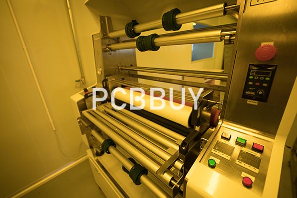
Development of high density and high frequency & development trend in PCB equipment
In the technology of through-hole processing of multilayer printed circuit board by layering method, the use of laser equipment has been practiced for more than 20 years. In 2000, the emergence of dual-beam CO, laser drilling equipment the development of this technology, so that the laser processing hole speed reached 1000 holes /s, than the initial laser drilling machine hole formation speed increased by about 10 times. At present, the development of new laser drilling machines continues to move in the direction of higher speed processing.
Using CO, laser drilling for hole processing aperture limit of 30 ~40 m. With the development of more fine-grained printed circuit boards, it is predicted that after 2022, UV laser equipment adapted to 20-50 m aperture processing will expand its scope of use. In the manufacture of printed circuit boards requiring aperture processing in the range of 30 to 40um, there will be CO, laser drilling machine as the first, and UV laser drilling machine as the second.
At present, the continuous development of multi-layer printed circuit boards containing filled holes with apertures below 50 m, the shape of the plating process holes and the guarantee of the thickness of the insulation layer are more closely dependent on the physical properties of the substrate material. It is predicted that in the next few years, in the substrate materials and later engineering, there will be new solutions to the above topics, and new substrate materials will also appear. In this way, the laser drilling opportunity faces another important issue, that is, how to cooperate with the new substrate material to achieve high accuracy in the position of the hole, and the high accuracy here refers to the accuracy control in the range of a few microns to 10m.
In terms of mechanical drilling equipment, the practical application of the ultra-high-speed spindle of 250,000 r/min has promoted the progress of mechanical drilling technology. It is predicted that extremely thin copper foil will be used to process multi-layer printed circuit boards and double-sided printed circuit boards with aperture above 100 m to improve hole quality and improve production efficiency as the main goal, and mechanical drilling technology will have great changes. This transformation is directly in competition with laser processing methods with machining apertures below 100um. In this technical competition, mechanical drilling equipment in the processing of 200pm aperture, narrow spacing, 150-200 m aperture requirements, must solve the problem of improving the quality of processing holes, improve production efficiency, improve metal ion migration resistance and other aspects. One of the important ways is to use high speed to reduce the cutting load.
It can be expected that with the advancement of the technology development of ultra-high speed spindle-using mechanical drilling methods can realize the processing of aperture 50~70um.
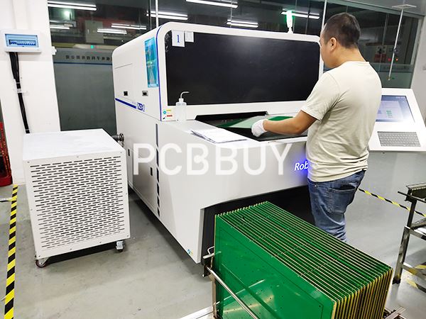
Due to the emergence and maturity of thin copper foil surface treatment technology, CO is directly used in double-sided printed circuit boards, and the processing of 70 ~100m through holes by laser drilling machine has become a reality, and after hole processing, it is generally necessary to remove the drilling dirt formed by laser drilling at the hole. In the future, with the development of laser drilling equipment technology and the application of substrate materials suitable for laser drilling, the post-processing process of this drilling process will be reduced.
The processing equipment with a pass-through hole aperture below 50 um is mainly used by UV laser machine. At present, the further development of the laser drilling equipment is mainly around the requirements of coordinating the quality of the hole and the processing speed.
Reference
He Wei, PCB Basic Electrical Information Science and Technology, China Machine Press,446-452
Industry Category


