What Is the Importance of PCB Error Analysis?
By:PCBBUY 02/21/2024 15:47

To start your checklist, start at the foundation of your PCB design and work your way through it. Some fundamental tasks must be done first to complete a successful layout, and you want to be sure to account for them. In fact, many PCB design departments will have multiple design reviews with different checklists for each review.
What are errors in PCB manufacturing? If you are curious about errors in PCB manufacturing, please check and read the content below for more information in this passage.
What Are the Main Errors in PCB Manufacturing?
Temperature & Moisture
PCBs are affected by temperature, both in storage, and when they are installed in components. Extreme temperatures or large temperature fluctuations may cause components or joints to break or fail. Many people take the maximum or minimum safe temperature into consideration, without thinking about the fluctuations in temperature that may occur either during operation or in storage. Exposure to moisture, both during the manufacturing process and in storage, can cause shorts to occur and may lead to defects in components. Humidity in the air, as well as the moisture content in the solder can wreak havoc on printed circuit boards, causing corrosion.
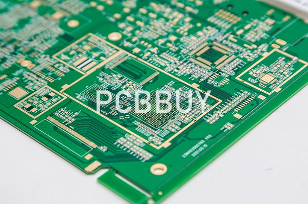
Plating Hole Defects
Holes carry electricity from one side of the board to the other. Plating of the hole wall during manufacture. During this, If the copper deposition is incorrect, it will create plating voids, leaving gaps in the wall with no copper coating. It could happen due to air bubbles, contamination in the holes, contaminated materials, and other similar reasons. You can prevent this from happening by following the manufacturer’s direction and cleaning the equipment as instructed.
Soldering Defects
The bulk of printed circuit board defects can be traced back to a soldering issue. Soldering is a technical skill that becomes even more difficult when dealing with the extremely small components on a printed circuit board. Some of the most common soldering defects include:
Open joints, sometimes called “dry joints,” occur when the solder doesn’t bond correctly with the point of contact, typically the pad. Occasionally, open joints are caused by using too much solder, which causes the component to lift.
Shifts occur when the printed circuit board or component is not aligned correctly during the soldering process. Shifts can result in open joints, shorts, and crossed signal lines. Short circuits, often referred to simply as “shorts,” most often occur due to a soldering error called solder bridging.

What Is the Importance of PCB Error Analysis?
As smart phones, tablets, and wearable devices have become smaller, thinner, and more functional, PCBs and components continue to be even smaller, denser, and more layered. In the automotive industry, research and development of technologies such as automatic brakes and autonomous driving has promoted computerized control of important components. Such control then expects PCBs and electronic components to have high durability and reliability so as to withstand long-term stress caused by driving, accelerating, and stopping.
Terminals and devices now have an important role in various daily situations, and cars require a high degree of safety. Any failures and defects of important components that are computerized in such products can lead to serious trouble or accidents.
To evaluate the durability and reliability of PCBs and electronic components, reliability evaluation tests, including acceleration tests, have become increasingly important. In addition to such tests, using microscopes to identify defects and failure causes is more important than ever.
What are the basics of avoid PCB error?
To start your checklist, start at the foundation of your PCB design and work your way through it. Some fundamental tasks must be done first to complete a successful layout, and you want to be sure to account for them. In fact, many PCB design departments will have multiple design reviews with different checklists for each review. These could include a pre-layout review, a component placement review, and a critical routing review, for example. All of these elements are included here and you can decide how best to organize the list, or lists, for your workflow:

Schematic
· Complete: Has the circuitry been completed in the schematic? It is a good idea to review the schematic prior to the layout to ensure that any missing circuitry is caught before the physical layout is started.
· Checked: Have all of the schematic design rule checks (DRCs) been run and any errors cleaned up?
· Ready for layout: Have all of the components been updated to their latest library versions? Many board designs have been ruined because the schematic still contained preliminary library parts instead of their final versions.
Board outline
· Correct documentation: Do you have the latest board information to work with? This would include mechanical dimensions, as well as connector and other mechanical part locations.
· Available data files: If you are working with mechanical CAD data that will be used in your PCB layout tools, are those 3D files ready and up to date?
· Board layer stackup: Do you have board layer stackup finalized with the correct configuration and materials? This is important for good signal integrity and manufacturability.
Industry Category


