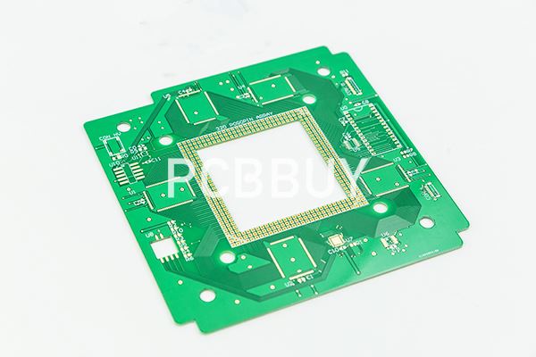
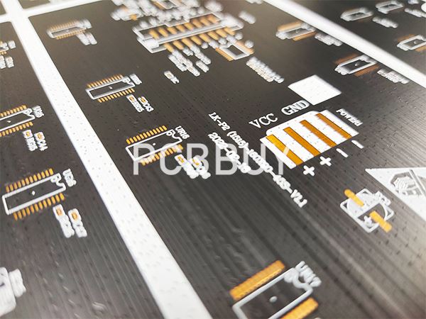
What Is the Key Process of HDI PCB Manufacturing?
By:PCBBUY 05/31/2024 17:43

With the rapid development of mobile communication technology, miniaturization, lightweight and high performance of devices such as personal computers, tablet computers, smart phones and wearable electronic products have become an inevitable development trend. The electronic components that constitute its fictionalization, including IC chips, PCB, passive electronic devices, etc., are promoting electronic products to achieve this goal. HDIion (HDI) laminated PCB uses the method of stacking to increase the density of planar and 2-way three-dimensional interconnection, so that multi-layer PCB can carry more signal interconnection.
As early as 1976, there were literature reports of PCB stacking methods, until 1991 IBM (Japan branch) published the stacking method caused many concerns, 1996 published the development of product report, since 1999 has formed a considerable scale of production, and rapidly applied to mobile phones. In particular, the use of resin-coated copper foil laminate has been popularized all over the world.
What Is the Basic Information of HDI PCB?
Compared with ordinary multi-layer PCB, high-density interconnected PCB achieve micro-size and high-density interconnection in three dimensions. Whether the product is a high-density interconnect laminated PCB can be judged from the following characteristics:
1) Containing micro-blind holes, buried holes, minimum aperture ≤$0.1mm; Hole ring ≤0.25mm.
2) The hole density of the micro-through hole is >600 holes /in2 (1in =25.4mm).
3) Trace width or spacing ≤0.10mm.
4) The wiring density (set the channel grid to be 0.05in) exceeds 117in/in
In the manufacture of HDI laminated PCB product, the micro through-hole technology depends not only on the manufacturing process of laminated PCB, but also on the selected media material. Therefore, the laminated multi-layer PCB can be divided into the following categories according to the type of medium material used in the base and the formation method of micro-conduction holes and the form of electrical interconnection:
(1) Classified according to the medium material of the laminated PCB
1) Laminated PCB made of photosensitive materials
2) Laminated PCB made of non-photosensitive materials
(2) Classified according to the formation process of micro through holes
1) Photoporous laminated PCB
2) Plasma porous laminated PCB
3) Laser hole laminated PCB
4) Chemical hole stacking PCB
5) Jet sandblasting perforated laminated PCB,
(3) Classified by electrical interconnection method
1) Electroplating method of micro-through hole interconnect multi-layer PCB.
2) Micropass-hole interconnect multi-layer PCB with conductive rubber plug method.
As mentioned above, there is no unified division and regulation of the type of high-density interconnect laminated PCB, and a more accurate, standardized and scientific classification method needs to be developed in the future research and production process according to the characteristics of laminated multilayer PCB.
What Are the Materials for HDI laminated PCB?
The materials used to implement the high-density interconnection of PCB should also have good electrical conduction and dielectric insulation properties under the condition of being light and thin.
1.Copper foil
According to IPC-4562 standard, copper roughness can be divided into the following four types according to the difference in R, as shown in Figure 13-1: When R>10m, copper belongs to HTE copper (standard copper); When 10pm>RzSum, the copper foil belongs to VLP copper foil (low profile copper); When 5pm>R2.5um, copper belongs to HVLP copper foil (ultra-low profile copper foil); When R<2.5um, copper belongs to FP copper (flat contour copper). Among them, EP copper is currently only in the research and development stage and has not been put into mass application. The market products are mainly HVLP and above grade copper foil.
For HDI laminated PCB, the roughness of copper foil is not only related to the fine line, but also has a great influence on the transmission loss and impedance of dry high frequency signal. The fineness of the circuit requires that the roughness of the copper foil must be low phase. In the current production technology, low-profile copper foil can be used for lines of about 100m, and to reach 50um lines, the roughness of the copper foil needs to be controlled at ultra-low profile scales.
2. Laminated resin material
The HDI laminated PCB is formed by multiple laminated processing, therefore, the resin material used in the laminated material must not only meet the requirements of light and thin, but also need to be able to withstand multiple lamination. In general, laminated resins are divided into two main process technology "branches" according to the presence or absence of fibers. According to these two branches, a review of the technological development of laminated resin materials in order of development time can be described in Figure 13-2. In the two branches and their various aspects, there has been great development and change in the past 20 years. This change is not only reflected in process technology, but also in material technology, product form, application and so on.
According to the comprehensive prediction of the basic characteristics, application processability, cost and other aspects of laminated resin materials, in the next few years in the laminated resin material market, Semi-curable organic Resin film substrate, Resin Coated CopperRCC substrate and glass fiber reinforced semi-curable sheet substrate suitable for laser processing of small aperture through holes will be the dominant substrate materials.
Most of the raw materials used in high-density interconnect laminated PCB are epoxy resin materials, such as according to the shape characteristics of the product manufactured by insulation materials and the formation of micro-conductive holes in the insulation layer, there are mainly three types of materials: photosensitive resin, non-photosensitive thermosetting resin and resin-coated copper foil.

The main types of photosensitive resins are liquid and dry film. The resin type of non-photosensitive thermosetting resin is mostly epoxy microfat, and the thickness of the resin insulation layer after curing is generally 40 ~60m. The resin coated copper foil for laminated PCB is composed of copper foil whose surface has been roughened, heat-resistant and anti-oxidation treatment, and copper foil (9~18um) semi-cured insulating resin is coated on the roughened surface. The resin layer (60~100um) as the resin layer of RCC, in addition to having the same manufacturing process as the FR-4 semi-cured phase coated resin copper structure, but also to meet the relevant performance requirements of the multilayer PCB, such as:
1. High insulation reliability and microthrough-hole reliability;
2. High glass transition temperature (T);
3. Low dielectric constant and low water absorption;
4. High bonding strength with copper,
5. Uniform thickness of insulating layer after curing.
RCC is a new fiberless product, which is conducive to laser and plasma etching treatment, and can better meet the lightweight and thin requirements of multi-layer PCB. In addition, the resin coated copper foil has a thin copper foil such as 12pm and 18um, which does not need to be coated with copper foil during processing, so the processing process is simpler. Copper foils in RCC are mostly electrolytic copper foils, but calendered copper foils can also be used according to the way in which resin-coated copper foil materials are combined on the laminated inner board to form an insulating layer, or the signal transmission characteristics of multi-layer PCB lines are required. Most of the insulating resins are epoxy resins, and a few also use polydiphenyl ether resin (PPE), polyimide resin (PI) and so on.
What Is the Key Technology of HDI Laminated PCB?
Manufacture of HDI laminated PCB core boards
Most of the original laminated multilayer PCB are manufactured using the core board method, that is, n layers on one or both sides of the conventional 0 circuit (before the general n=2 ~4) and the degree of 4-compound. A single, double-sided, or multi-layer PCB with medium layers is called the core board of a high-density interconnected PCB. Most of the laminated multi-layer PCB use fully through holes or have a buried hole, blind hole, through hole combination structure to improve the interconnection density, and even use a multi-layer PCB core board containing a core structure. In general, the manufacturing of core boards is mostly the use of existing PCB) raw materials, equipment and production technology. Obviously, the density of the core board is much lower than the density of the laminated multi-layer PCB, and its aperture is generally greater than 0.2mm, the line width and spacing are greater than 0.08mm, and the number of layers is mostly 2 to 6 layers. The 1~4 layers on one side or two area layers of the core board are higher density guide layers, whose hole diameter is less than 0.1mm, line width and spacing are less than 0.75mm. At present, if the above two densities are combined to form a laminated multilayer PCB, it can meet the requirements of very high density chip-level packaging and other forms of assembly.
HDI laminated PCB core board not only plays the role of rigid support of the laminated layer, but also plays the role of interconnecting with the physical storage and gas between the laminated layer, and it also plays the role of heat conduction (transfer). Therefore, in order to have one or two solid layers on the core board, in order to maintain the flatness of the screen body and the reliability of the electrical connection, the core board must be properly treated. Such as the board through the hole and the lining of the case, the surface treatment of the flat (wipe or board), the surface treatment of chemical copper and electroplating copper and the manufacture of conductive graphics.
Hole processing
HDI laminated PCB online is mainly characterized by machining blind holes. The blind holes of non-photosensitive thermosetting resin layer and resin-coated copper foil layer were processed by laser. For the photosensitive insulating resin, the blind hole is made by UV (ultraviolet) light through masking exposure and development.
There are Nd: YAG lasers in CO, laser and UV fields, all suitable for laser processing of resin layers. Due to CO, laser processing has obvious advantages in performance and speed, so its application has been popularized. UV-YAG laser is suitable for micro through hole processing and is expected to be popular in the future. CO, laser processing is achieved by thermal ablation, but the large amount of heat accumulated by thermal ablation is easy to separate the resin from the copper foil, so it is necessary to pay attention to the setting of processing conditions.
CO, laser cannot directly ablate copper foil, so when coating resin copper foil laser processing, first by etching copper into a copper window and then through the copper window for laser processing. The position and aperture of the hole processed by this method are restricted by the mask, and the porosity in the lower part of the mask is easily overstretched due to excessive light ablation, which leads to the reliability of the hole interconnection. In order to solve this problem, a CO, laser direct ablation processing technology is developed, which does not need to make copper window. However, before CO, laser direct processing, the copper foil must be blackened or browned before the surface.
Bonding of insulation layer
Both resin-coated copper pins and semi-cured copper-coated laminates face the problem of bonding between conductive copper patterns and resins. The lines of high-density interconnect laminated PCB are fine, so the lamination binding force is higher than that of ordinary multilayer PCB to prevent problems such as short circuit or signal interference between the lines.
Therefore, on the one hand, it is required that the cleanliness of the surface during the manufacturing process is not therefore, for high-density interconnect laminated PCB, high to reduce the impact of external factors on its electrical properties: on the other hand, it is also necessary to coarser the copper foil and chemical hydrophilic treatment through Browning technology, so that the copper surface forms a rough state. In order to achieve mechanical occlusion with resin material during lamination, the surface state changed from poor hydrophilic to better hydrophilic after Browning, thus improving the lamination bonding property. The surface coarsing problem of copper foil will affect the accuracy of the graphics in the production of hyperfine lines (<50um), and increase the loss of signal transmission and the impedance value of the signal transmission line. In order to solve this problem, ultra-coarsening technology and non-etching surface bonding enhancement technology have been gradually developed to meet the requirements of the continuous development of high-density interconnected PCB to miniaturization.
Electroplating and graphic production
In the manufacturing process of HDI laminated PCB, blind hole electroplating and even blind hole copper filling are required. Therefore, in the selection of electroplating process, the laminated PCB mainly selects the whole board electroplating technology. The blind hole electroplating process is accompanied by the continuous thickening of the surface copper layer. In the early electroplating solution technology is not very mature period, it is necessary to complete the blind hole electroplating or copper filling after the surface copper layer micro-corrosion to achieve the target thickness. However, the existing electroplating technology has gradually matured, and the blind hole electroplating copper or copper filling process is directly carried out on the basis of 9um or 12pm thin copper, and the surface thickness can be increased by only a few microns, thereby avoiding the instability of the process caused by secondary micro-corrosion
Connections between layers
The interlayer interconnection in the stacking method is realized through the multi-layer connection of the hole. Different forms of blind hole stacking, staggered blind hole stacking to form a through hole, the structure of the wiring density is lower, the electrical performance is also relatively low, so the current blind hole stacking mainly uses the through structure. Using the filled through holes in the filling holes of the plating company, the plating column method of deposited coating is realized by PRC(periodic reverse current) method or plating additives. The cylindrical coating pattern of the through holes is formed by graphic plating and semi-addition plating. It is a stacked pass hole with overlapping pass holes on the pass hole, and uses insulating resin or conductive adhesive to fill the inside of the blind hole of the figure. The laser passes through the conductor layer, and the hole is filled with a funnel-shaped through hole.
Surface treatment of pad
The surface treatment of the finished laminated PCB is important for component welding, trace bonding and convex connection of ball grid array (BGA). The surface treatment includes flux, hot air leveling solder coating, N/Au coating, etc., which can be selected according to the use, of which Ni/Pd/Au coating is the best. Due to the problem of electroplating traces in Ni/Pd/Au plating, a large number of replaced or reduced electroless Ni/Pd/Au plating are used in production to achieve the surface treatment of laminated PCB pads.
Reference
He Wei, PCB Basic Electrical Information Science and Technology, China Machine Press,282-286
Industry Category


