What Is the PCB Minimum Pad to Pad Spacing?
By:PCBBUY 03/30/2022 09:49

As far as the processing capability of mainstream PCB manufacturers is concerned, if the hole diameter of the pad is mechanically drilled, the minimum is not less than 0.2mm. If laser drilling is used, the minimum is not less than 4mil. The aperture tolerance is slightly different depending on the plate. Generally, the control can be within 0.05mm, and the pad width should be at least 0.2mm.
In this passage, we will tell you everything about PCB pad to pad spacing. If you are searching for more information about PCB pad to pad spacing, please check and read the content below for professional information.
What are the problems of incorrect PCB Pad size?
The size, shape, and position of a pad in a PCB footprint is tied directly into how well the circuit board can be manufactured. Using a pad that is incorrectly sized or out of position can cause different problems during the soldering processes used for PCB assembly. Here are some examples of those problems:
Floating parts: If a surface mount part is sitting on pads that are too large or spaced incorrectly, the part may float out of position during solder reflow. This can lead to the solder bridging over to other metal and insufficient component spacing for thermal cooling, rework, and PCB test.
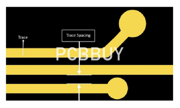
Incomplete solder joints: Pads that are too small or spaced too closely together may not allow enough room for a sufficient solder fillet to form. This can leave the part with a bad solder connection or no solder joint at all.
Solder bridging: As we discussed above, surface mount pads that are too large can allow a part to float, which could lead to solder bridging. This is where the solder crosses over to a pad or metal feature on another net and creates a direct short. Solder bridging can also happen if the correct solder mask and solder paste features are not designed into the pad shape in the CAD tools.
Tombstoning: When a small, discrete surface mount part is thermally unbalanced during solder reflow, the solder paste on one pad may melt faster than on the other and pull the part up in a vertical, or “tombstone,” position. This is usually the fault of one pad being connected to a large metal plane that acts as a heat sink, but it can also happen if inconsistent pad sizes are used between the two pins.
Solder wicking: While the problems discussed so far have belonged to surface mount pad shapes, thru-hole pads can also experience difficulty if not constructed correctly. If too large of a drill size is used for the component lead going into the hole, the solder may wick down through the hole before making a good connection. On the other hand, a drill size that is too small will make inserting the component lead difficult and slow down assembly.

Why PCB Pad size standards are important?
First of all, let’s define exactly what a “pad” is. A pad, also known as a “land,” is the exposed area of metal on a circuit board that the lead of a part will be soldered to. Multiple pads are used to create the component footprint, or land pattern, on the printed circuit board.
This process could be very error-prone, however, as manufacturers’ specifications didn’t always adhere to the same formulas. This could result in layout designers using the wrong sizes and shapes in their pads. These incorrect pad sizes and shapes, unfortunately, could have disastrous consequences during manufacturing, including:
Through-hole breakout: Through-hole pads must have a solid annular ring for solderability, which is the metal between the hole wall and the outer perimeter of the pad. The annular ring specification is designed to be large enough to allow for the expected amount of drill wandering from the center of the hole. If the pad is too small, however, there could be some breakout of the annular ring, and too much breakout can result in improper soldering or broken and incomplete circuits.
Insufficient solder joints: SMT parts that have too small of pads run the risk of not getting a proper solder fillet during manufacturing. Without a good fillet, the solder joint will be weak and can break.
Floating parts: SMT parts that are soldered to pads that are too large could end up floating out of position during solder reflow. This can cause conflicts with other parts or even shorts between circuits.
How to design PCB Pad to Pad spacing?
Of course, you must get all of your parts on the board, and you probably have already done a space study to ensure your parts will fit. If for some reason the parts don’t fit due to mistakes in package types or sizing, added features, or reduced board size, then you will have to rethink the design and come up with some ways to reduce the circuitry. But at this point in the design, there’s probably enough room for the parts. The concern now is coming up with the optimum component placement for the best design functionality.

Sensitive components may need a specific amount of spacing in relation to other components to reduce the chance of signal interference. Differing areas of circuitry, such as analog versus digital, will also need precise spacing between them. In addition, parts that run hot will need space for cooling, and you will need to allow yourself enough room for routing. On the flip side, components that are part of high-speed signal paths, power converters, or other sensitive circuits must be placed close together.
All of these needs can cause pad-to-pad spacing problems for you if you aren’t careful. Some designers will shrink their pads to create more room around them, or they will squeeze them together to save space or reduce signal length. Both of these conditions can create problems during manufacturing. To avoid this, you need to follow the industry-standard rules for component footprint creation and parts placement. Let’s look at some of the problems that can arise from inadequate pad-to-pad spacing if the rules aren’t followed.
Industry Category


