What Is the Principle Blind Vias of PCB?
By:PCBBUY 12/23/2024 14:52
Printed Circuit Boards (PCBs) are the backbone of modern electronic devices, offering a platform for electrical connectivity and mechanical support for components. One of the advanced techniques in PCB manufacturing involves the use of blind vias. These specialized vias have revolutionized PCB design and functionality, particularly in high-density and high-performance applications. This article delves into the principles, process, advantages, functions, and impacts of blind vias on PCB manufacturing.
What Is the Principle of Blind Vias?
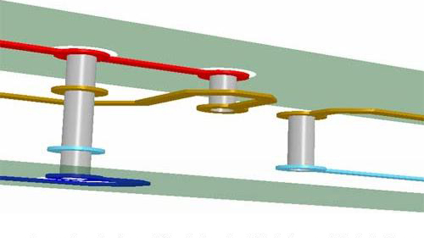
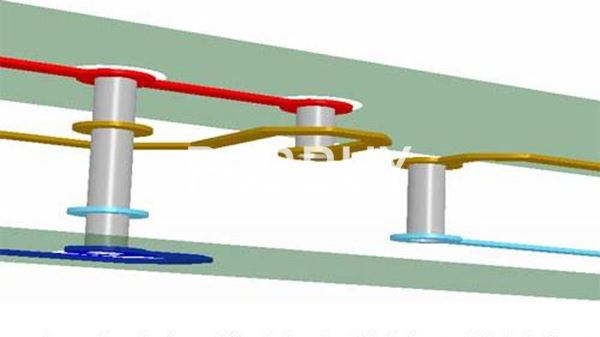
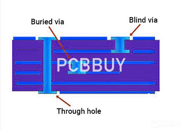
A via in online PCB terminology is a pathway that allows electrical connection between different layers of a PCB. Traditionally, vias are categorized into through-hole vias, blind vias, and buried vias. Blind vias are distinctive because they connect an outer layer of the PCB to one or more inner layers but do not pass through the entire board. This feature allows designers to optimize space on the PCB, which is crucial in complex, multi-layer boards.
Design Parameters
|
Aspect Ratio |
Ø min. |
Ø max. |
Via Pad |
Annular ring min.* |
|
|
Blind Via (mechanical) |
1:1 |
200µm |
300µm |
400µm |
100µm |
|
⇒ as Special production |
1:1.2 |
150µm |
150µm |
350µm |
100µm |
|
Blind Via (laser) |
1:1 |
100µm |
100µm |
280µm |
90µm |
What is the Process of Creating Blind Vias?
The manufacturing of blind vias involves several meticulous steps, each ensuring precision and reliability. The process can be summarized as follows:
1. Drilling: The creation of blind vias begins with drilling. Unlike through-hole vias, blind vias require controlled-depth drilling to ensure they only penetrate to the required inner layer. This can be achieved through mechanical drilling or more advanced laser drilling. Laser drilling is often preferred for its precision, especially in high-density interconnect (HDI) PCBs.
2. Copper Deposition: Once the holes are drilled, they need to be electrically conductive. This is achieved through a process called electroless copper deposition. A thin layer of copper is deposited on the walls of the vias, creating an initial conductive layer.
3. Plating: The initial copper layer is then thickened through electroplating. The board is submerged in an electrolytic bath, and an electric current is passed through it, causing additional copper to deposit on the via walls. This step ensures that the vias are robust and capable of carrying the necessary current.
4. Surface Finish and Etching: After plating, the PCB undergoes surface finishing and etching processes to define the circuit patterns. This step also includes applying solder masks and other protective coatings to ensure durability and performance.
5. Inspection and Testing: The final step involves rigorous inspection and testing to verify the integrity and functionality of the blind vias. Techniques such as X-ray inspection and electrical testing are employed to detect any defects or discontinuities.
What Are the Advantages of Blind Vias?
Blind vias offer several significant advantages over traditional through-hole vias:
1. Space Optimization: By connecting only specific layers, blind vias free up valuable surface real estate on the PCB. This allows for more components to be placed on the board, facilitating miniaturization.
2. Improved Signal Integrity: In high-speed digital and RF applications, blind vias reduce signal path lengths, thereby minimizing signal degradation and electromagnetic interference (EMI).
3. Enhanced Reliability: With fewer interconnections traversing the entire board, there is a reduced risk of mechanical stress and potential failure, enhancing overall multilayer PCB reliability.
4. Layer Management: Blind vias allow for more efficient layer management, particularly in HDI PCBs, where they can be used to create complex interconnections without increasing board thickness.
What Are the Functions and Applications?
Blind vias are essential in several advanced applications, including:
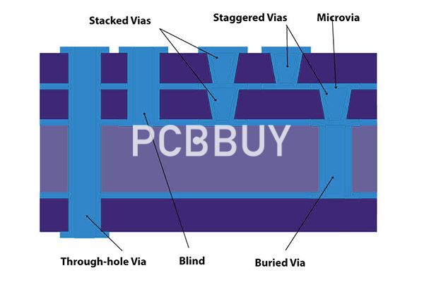
1. HDI PCBs: High-Density Interconnect PCBs leverage blind vias to achieve higher wiring density, crucial for smartphones, tablets, and other compact electronic devices.
2. RF and Microwave Circuits: These circuits benefit from the reduced inductance and capacitance that blind vias offer, ensuring better performance at high frequencies.
3. Medical Devices: Miniaturization and reliability are critical in medical electronics, where blind vias enable the creation of compact, yet highly reliable PCBs.
4. Automotive Electronics: In the automotive sector, where space constraints and robust performance are essential, blind vias play a pivotal role in advanced driver-assistance systems (ADAS) and infotainment systems.
What Is the Impact on PCB End-Product?
The integration of blind vias in PCB design significantly impacts the final product in several ways:
1. Miniaturization: Products can be made smaller without compromising functionality, thanks to the efficient use of PCB space facilitated by blind vias.
2. Performance: The electrical performance of the PCB is enhanced due to shorter and more direct signal paths, which is critical for high-speed and high-frequency applications.
3. Complexity Designers can create more complex and feature-rich PCBs without increasing the number of layers or the overall size of the board.
4. Cost: While the initial manufacturing cost may be higher due to the specialized processes involved, the long-term benefits of increased reliability and performance can offset these costs.
Blind vias are a powerful tool in the arsenal of PCB designers and manufacturers, offering a means to optimize space, improve performance, and enhance reliability in complex electronic devices. As the demand for smaller, faster, and more reliable electronics continues to grow, the use of blind vias is set to become even more widespread, driving innovations across various industries. Understanding the principles, processes, and advantages of blind vias is essential for anyone involved in the design and manufacture of modern PCBs.
What Are the Differences among the 3 Types of Through-hole Vias?
There are three types of through-hole vias that we often see, as follows:
Plating Through Hole, referred to as PTH
This is the most common type of via, and you can identify it by holding the PCB up to a light source,the holes that allow light to pass through are the plating through holes. This is also the simplest type of via to produce, as it can be made by drilling or laser-cutting holes directly into the circuit board, and is relatively inexpensive. However, in some cases, certain layers of the circuit board may not require connections through these PTHs. For example, if I bought the third and fourth floors of a six-story building and wanted to design an internal staircase connecting only the third and fourth floors, the space on the fourth floor would be wasted by the staircase connecting the first floor to the sixth floor. Therefore, while PTHs are inexpensive, they can sometimes take up additional space on the PCB.
Vias are also divided into PTH and NPTH.
Blind Via Hole, referred to as BVH
Blind via are used to connect the outer layer of PCB circuits to adjacent inner layers via electroplated holes. Because the opposite side cannot be seen, it is called a blind via. This manufacturing process is used to increase the utilization of space for PCB circuit layers. However, special attention must be paid to the depth (Z-axis) of the drilling, as it can often cause difficulties with electroplating the inner space of holes and thus is almost no longer used by manufacturers. It is also possible to drill the necessary connecting holes in individual circuit layers during the manufacturing process and then bond them together at the end. For example, in a 2+4+2 layer board,you can drill the outermost two layers first,or the 2+4 layers can be drilled simultaneously, but this requires more precise positioning and alignment equipment.Take the example of buying a building above as an example. In a six-story house, there are only stairs connecting the first floor to the second floor, or connecting the fifth floor to the sixth floor, which are called blind via.
Buried Via Hole referred to as BVH
Buried via holes connect two or more inner layers without reaching the outer layer. This process cannot be achieved by drilling after bonding, and requires partial bonding of the inner layers, followed by electroplating treatment, before final bonding can be completed. It is more time-consuming and expensive than making plating through holes or blind via, and is typically used for high-density (HDI) circuit boards to increase available space for other circuit layers. Using the analogy of buying a building, when only the stairs between the third and fourth floors are connected in a six-story building, it is called buried via holes. Buried via holes cannot be seen from the appearance of the board and are actually located in the inner layers of the circuit board.
Reference
He Wei, PCB Basic Electrical Information Science and Technology, China Machine Press,120-122
Industry Category


