What Is the Process of HDI PCB Manufacturing?
By:PCBBUY 11/27/2024 16:37

A HDI PCB is usually found in complex electronic devices that demand excellent performance while conserving space. Applications include mobile /cellular phones, touch-screen devices, laptop computers, digital cameras, 4/5G network communications, and military applications such as avionics and smart munitions.
In this passage, we are providing all the knowledge of HDI PCB, please check and read the content below for more information.
What is the Market Situation of HDI PCB?
Before we head into forecasts, let’s mention current statistics. It doesn’t take an expert to see that the printed circuit boards are trendy throughout the world. You can even find guides explaining how to make a PCB at home.
However, if you want to launch a commercial product, it is vital that you design and assemble a reliable PCB, and you need professional equipment and experts for that.
The PCB industry has recently set a new standard in high-density to interconnect technology (HDI). Users throughout the world have accepted it and implemented it in their products and other applications.
A report published by expert’s pinpoints that this market earned more than $9.4 billion in 2017. The estimation is that the compound annual growth rate (CAGR) will be over 11% in the coming years. If you do the math that means that the HDI PCB market can generate more than $22 billion by 2025!
That is not only 2.5 times more than the result made in 2017, but it is also an achievement that will positively surprise the entire industry. And the best part is that it seems more than feasible, especially if we consider the fantastic progress the sector made in only a couple of years.
Even if the growth is somewhat less than projected, There is no doubt that the high-density interconnect PCB market will usher in a bright future. The technology hasn’t reached its peak yet, which means we can expect even better boards in the coming years. On top of that, more companies are joining the production of HDI boards every day, increasing their use.
Why HDI PCB is popular?
If we analyze the situation from 2017, we can notice that about 66% of the total HDI PCB revenue was for the tablet and smartphone industry. That makes sense because these products require a high-performing board that will be thin and compact-sized at the same time.
The experts do not doubt that smartphones and tablets will remain the most popular HDI PCB application in the coming years. They should keep the leading position for at least five years from now, but the exciting thing to discuss is the growing popularity of other smart products.
We are talking about smartwatches and other wearables with “smart” features. All those products are electronic devices, and they require printed circuit boards to work. As a result, the PCB industry has been producing significantly more for this application.
The estimated annual growth rate for PCB use for smart wearables is around 14% in the coming years. Although smartphones and tablets will remain at the top, watches and other wearables will get closer by 2025.
What is the process of HDI PCB manufacturing?
There are a number of steps involved in the typical PCB manufacturing process, but HDI PCB manufacturing uses some particular steps that may not used in other boards. The HDI design process starts like many other processes, where the
· Determine the layer count required to route all signals, either by using the largest BGA component on the board or by using the interface + direction count from the largest IC on the board.
· Contact your fabrication house to select materials and obtain dielectric data to create your PCB stackup.
· Based on layer count and thickness, determine the via style that will be used to route signals through inner layers.
· Perform a reliability assessment if relevant, to verify that the materials will not stress interconnects to fracture during assembly processing and operation.
· Determine design rules based on fabricator capabilities and reliability requirements (need for tear drops, trace widths, clearances, etc.) to ensure reliable manufacturing and assembly.
Stackup creation and determination of design rules are the critical points as they will determine ability to route the board and reliability of the end product. Once these points are completed, a designer can implement their fabricators DFM requirements and reliability requirements as design rules in their ECAD software. Doing this on the front-end is very important and it will help ensure the design is reliable, routable, and manufacturable.
1. Design and Stack-Up Configuration
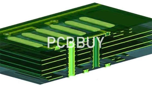
HDI boards employ unique stack-ups, such as 1+n+1, 2+n+2, and more, denoting the number of HDI layers surrounding the core.
2. Laser Drilling
High-precision lasers create microvias with diameters as small as 50 μm.
3. Sequential Lamination
Sequential build-up (SBU) layers are added one at a time, with vias plated between each layer.
|
SBU Type |
Layers |
Applications |
|
1+n+1 |
Single HDI |
Smartphones, tablets. |
|
2+n+2 |
Double HDI |
High-performance networking. |
4. Surface Finishing
Common finishes include ENIG (Electroless Nickel Immersion Gold) and OSP (Organic Solderability Preservatives).
Applications of HDI PCBs
High-Density Interconnect (HDI) PCBs have become indispensable across various industries due to their high performance, compact size, and the ability to support complex designs. These boards utilize advanced features like microvias, smaller pads, and finer lines to enable greater functionality in a reduced physical space. Below are some of the key areas where HDI PCBs are applied:
1. Consumer Electronics
In the consumer electronics sector, HDI PCBs are used extensively in mobile devices, such as smartphones, tablets, and wearables, to enable faster data transmission and greater functionality in smaller packages.
-
Smartphones and Tablets: These devices require HDI PCBs for their compact design, supporting high-frequency signals, fast processing, and multi-layer connections. HDI PCBs provide the necessary bandwidth for 4G, 5G, and Wi-Fi connectivity, making them essential for modern mobile devices.
-
Wearables: Smartwatches and fitness trackers leverage HDI PCBs for miniaturization, allowing more sensors and features to be packed into smaller sizes without compromising performance.
2. Automotive Industry
The automotive sector relies on HDI PCBs for various applications, including in-vehicle electronics, infotainment systems, and advanced driver-assistance systems (ADAS).
-
ADAS: HDI PCBs are used in the critical electronics for systems like lane assist, parking sensors, and adaptive cruise control. These systems require high-speed, high-density interconnects to process vast amounts of data in real-time.
-
In-Vehicle Electronics: Infotainment, climate control, and navigation systems benefit from the miniaturization offered by HDI technology, reducing the space required while improving functionality and reliability.
3. Aerospace and Defense
HDI PCBs are crucial in the aerospace and defense industries due to their reliability, compactness, and performance at high frequencies and temperatures.
-
Satellites: Satellite communication systems require HDI boards to ensure efficient and stable operation in harsh environments. The ability to integrate high-performance components in limited space makes HDI an ideal choice.
-
Avionics: HDI PCBs are used in avionics systems, where reliability and precision are essential for navigation, communication, and control systems.
4. Medical Devices
The healthcare industry benefits significantly from HDI technology, especially for devices that require miniaturization and reliability.
-
Portable Diagnostics and Monitoring: Wearable medical devices, such as continuous glucose monitors, ECG devices, and smart insulin pumps, rely on HDI PCBs to integrate multiple functions into a compact, user-friendly device. These PCBs ensure high-speed data processing and low power consumption, which are vital for medical applications.
-
Implantable Devices: HDI PCBs are also used in implantable devices, where small size and durability are critical. These devices, such as pacemakers and neurostimulators, require HDI PCBs to withstand the body's environment while ensuring consistent operation.
5. Telecommunications
With the rise of 5G, the telecommunications industry demands high-density interconnects for faster speeds, lower latency, and enhanced capacity. HDI PCBs support this need by enabling the integration of advanced technologies in communication systems.
-
Base Stations and Network Equipment: HDI PCBs are used in telecom infrastructure, where high-frequency performance is required for base stations, routers, and switches. Their compactness helps optimize space within equipment while maintaining high performance.
-
5G Devices: HDI PCBs are vital in the production of 5G-enabled devices. These devices require complex, high-speed circuitry that can handle the increased data rates, and HDI technology provides the compact, high-density solutions needed.
6. High-Performance Computing
In high-performance computing (HPC) systems, such as servers, workstations, and supercomputers, HDI PCBs are used to meet the demands of faster processing and high-volume data transfer.
-
Servers and Data Centers: These systems require HDI boards to accommodate advanced processors, memory chips, and other high-speed components in a limited space, ensuring that performance is maximized while minimizing power consumption and thermal issues.
-
Graphics Processing Units (GPUs): HDI technology enables the production of powerful GPUs for gaming, AI, and scientific applications, where high-speed data transmission and dense circuit layouts are essential.
Conclusion
HDI PCBs are essential in a wide variety of industries where miniaturization, performance, and reliability are paramount. From consumer electronics to automotive systems, aerospace applications, and high-performance computing, HDI technology enables the design of complex circuits within small, high-density footprints. As technology continues to evolve, the demand for HDI PCBs will only increase, making them a cornerstone of future electronic innovation.
Industry Category


