What Is the Process of Making Presensitized PCB?
By:PCBBUY 03/02/2024 16:29

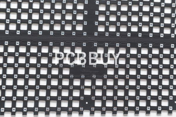
Presensitized PCBs have numerous benefits, making them the number one choice of most manufacturers and engineers. A presensitized PCB is a special type of PCB where the surface of the board contains a unique photo-sensitive material coating. This presensitized PC board makes it easy for you to apply your unique custom design by transferring (or “burning”) the image by using UV lights.
Do you know the methods of making presensitized PCB? If you are curious about the process of making presensitized PCB, please check and read the passage for more information.
What Is the Process of Making Presensitized PCB?
A presensitized circuit board is a special board with a photosensitive surface coating. It enables you to create a customized design by shifting/burning the image with a UV light. In other words, a presensitized circuit board resembles a standard copper-clad board. The only difference between them is how you transfer the design into the boards.
Here are the steps of making presensitized PCB:
PCB Artwork
Remember to scrutinize your tracing paper before utilizing it. Light up one part of the paper with a shiny source of light, and examine it by viewing through the other side. The paper should be free from dark spots and stains. Dark spots cover the artwork portions, forming short circulating pathways around crowded sections of the board artwork.
PCB Printing
You should use laser-made positive artwork in your PCB printing exercise as they form delicate, crisps, and compact black prints. Inkjet inks seam to stain with tracing paper, resulting in prints with draining and blurry edges. Consequently, this limits the feasible spacing between circuit board pads and traces.
PCB Preparation
It is essential to realize that a presensitized board surface is shielded with a dense grey layer against unintended exposure and impurities. You will use the extended part later to attach your PCB standoff clip during the design and etching process. Burrs and uneven edges may limit your artwork from lying ideally uniform.
PCB Exposure
First, clean your exposure box surface with a cloth containing a mild detergent. Then, rinse it with a clean, dry cloth. Take out the protective PCB layer. Thirdly, gently slide your board in between the upper and lower artwork. Fourthly, insert the board in the exposure box. Expose Your PCB for 8 Minutes then fit the Standoffs, finally drip the PCB in Developer Medium.
PCB Etching
PCB etching is an important step in the chemical preparation of presensitized PCBs. It involves the removal of copper to obtain desirable patterns. Remember, you need to do away with every copper residue apart from the circuitry covered by the tin plating.
PCB etching seems to be a complicated process for some people, but actually, it is not a challenging activity, as you may think. After collecting all the necessary materials, print your layout before printing the circuit layout. Sketch your design in transparent acetate material to achieve the desired results.

PCB Exposure
The UV-light exposure box needs to be set up. It is a move that will help block UV rays from crossing the black lines of your design. After that, have your first artwork carefully attached with tape to the pane. Subsequently, carefully add the remaining designs, which will help with the overall opacity.
Once completed, you will have to work with a photosensitive resin, a task that may compel that your workplace is an area with reduced brightness.
With a lot of caution, peel off the PCB’s protective film while placing the sensitive sides into place, not forgetting to steadfast it on a site using tape. Make sure you put them all into the exposure box with the delicate side-facing UV tubes. Don’t forget to seal it.
PCB Development
With this step, place your PCB as soon as possible into a bath made of sodium hydroxide with the sensitive part facing up. Then immediately, a blue-purple color appears and sometimes might be grey.
Gently shake the bath so that the design is visible at around 30” to 60”. After that, place the PCB in the water bath and wash it.
Engraving Your PCB
Here, the photosensitivity of your PCB is not minimal, and you can confidently switch the lights on. After this, carefully ensure that you place your PCB copper in an upward position into the FeCI3 acid bath while gently swirling it.

The solution needs to be in motion to enable the reaction to occur. At around 20’ to 40’ –depending on the water bath’s temperature, the copper’s surface area will dissolve. Such takes place immediately; remove your PCB, rinse it to a separate water bath, and then let it dry out.
Washing of your PCB
The remaining resin that was stuck onto the circuit needs some scrapping. But to easily do that, you will have to place the PCB slowly in an acetone bath, and if you are keen enough, you’ll notice the acetone turning to become yellow.
Industry Category


