What Is the Role of PCB Copper Balance in Manufacturing?
By:PCBBUY 11/28/2024 17:23
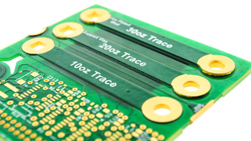
Printed Circuit Boards (PCBs) are the backbone of modern electronics, enabling the connection and functionality of components in devices ranging from smartphones to aerospace systems. Among the critical aspects of PCB design and production is copper balance, a factor that significantly impacts the structural integrity, electrical performance, and manufacturability of a PCB. This article explores the concept of copper balance, its importance in PCB manufacturing, the principles guiding its implementation, and the challenges involved.
What is PCB Copper Balance?
PCB copper balance refers to the even distribution of copper across a PCB's layers during the manufacturing process. An imbalance occurs when copper is disproportionately distributed, leading to issues such as warping, uneven etching, and reduced reliability of the final product.
Key considerations in copper balance include:
-
Uniform Etching: Maintaining copper distribution prevents over-etching or under-etching during chemical processing.
-
Thermal Stability: Uneven copper layers may cause thermal expansion discrepancies, leading to warping.
-
Mechanical Strength: Proper balance enhances the structural durability of the PCB.
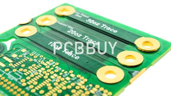
Importance of Copper Balance in PCB Manufacturing
Prevention of Warping and Bowing
Excessive copper on one side of the PCB can lead to mechanical stress during heating, causing bending or warping.
Warping tolerance for PCBs in critical applications is typically below 0.75% for multilayer boards.
Improved Electrical Performance
Uniform copper ensures stable impedance, critical in high-frequency designs.
Copper imbalance can cause unexpected variations in electrical properties, affecting signal integrity.
Efficient Manufacturing Processes
Balanced copper improves yield rates by minimizing defects during drilling, etching, and lamination.
What role does PCB copper balance play in PCB manufacturing?
The manufacturing of the copper traces of your board, whether on the surface or for internal layers, is done by etching, one of the major PCB manufacturing steps. Layer fabrication begins with a laminate sheet that is completely covered by copper. Etching is the process of removing excess copper from traces and other areas, such as component pads and annular rings for vias, using an ammonia-based solution.
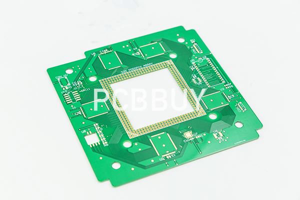
One of the vital design specifications to be followed is the ‘copper balance’ in the PCB Fabrication. The consistent copper coverage in each layer of the PCB stack-up has to be achieved to avoid electrical and mechanical issues that can impede the circuit performance.
Copper balancing is a method of symmetric distribution of copper traces in every layer of the PCB stack-up. This is necessary to avoid concerns of board twists, bow, or warpage. Layout engineers and fabricators insist on the mirrored stack up with the top half layers to be exactly symmetric with the bottom half layers of the PCB.
Copper is an integral part of any PCB design as it has exceptional electrical and thermal characteristics necessary for signal transmission and heat dissipation.
· Copper used as traces transfer heat along with signal across the board. This decreases the damage caused by irregular heating of the board that may lead to internal track breakage.
· Copper used as a heat sink layer for power generating circuits avoids the usage of extra heat sink components and reduces the manufacturing costs to a good extent.
· Copper used as a plating on the PCB increases the conductor and surface pad thickness. Also, a strong inter-layer copper connection is achieved through plated through holes.
In PCB Fabrication, if there is an uneven distribution of copper among the stack-up layers then the following mechanical alignment issues can occur.
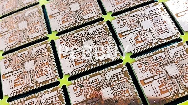
· Twists: The vertical displacement of one corner that is not in the same plane as compared to the remaining three corners of the board is known as the twist in the PCB.
· Bow: A spherical or cylindrical curvature of the PCB while the four corners of the board are in the same plane is said to be the Bow issue of the board.
· Warp: Any unintended change in the PCB shape is known as Board Warping in general. The high temperature and pressure of the fabrication process itself can cause warpage which is also known as the “Potato chip” effect in PCB Fabrication. The warped boards can stress the traces or solder joints which might further lead to damaged circuits.
· Bow and Twist issues also depend on the technical characteristics of a PCB like board thickness, type of substrate materials, etc. Thin boards get warped frequently while going through high-temperature fabrication processes. Selecting the right type of material and correct PCB thickness can help in reducing the mechanical issues to a good extent.
PCB Copper balance plays a significant role in PCB fabrication and component assembly. Even distribution of copper in each layer and across the entire stack up is important to avoid issues of the bow, twist, and warping of PCB.
If stack-up is not balanced, along with bow and twist issues there can be variation in the overall PCB thickness. Uneven copper coverage in different layers can lead to mismatched thickness on each side of the board after the lamination process.
How to process PCB copper balance?
Printed circuit boards (PCBs) consist of insulating substrates upon which tiny copper tracks and electrical components are placed. The thickness value of a copper track is often expressed in copper weight. A copper weight of one-quarter oz. corresponds to a thickness of .00036 inch. Modern-day PCBs are often double-sided; when this is the case, similar thicknesses and amounts of copper should be placed on each side. This process is known as copper weight balancing.

Create a new CAD project. Create three CAD layers. By convention, layer 0 is the board outline. Draw the board outline in layer 0.
Draw the copper tracks of the front side of the PCB and place them in CAD layer 1. Calculate the area of copper that is taken up on the front side of the PCB. This can be done by multiplying track width by track length for each track.
Draw the copper tracks on the back side of the PCB and place them in CAD layer 2. To balance the copper, try to keep the track area on the back side similar to the track area on the front side. When sending the CAD design to the manufacturer, specify the same copper weight for both sides of the board.
Chemical and Physical Principles of Copper Balancing
Copper balancing leverages principles of material science and chemistry. During fabrication, etching solutions like ferric chloride (FeCl₃) are used to remove unwanted copper. The reaction can be summarized as:
2FeCl3+Cu→2FeCl2+CuCl2
This process requires precise control, as uneven copper thickness leads to differential etching rates. Balancing copper involves designing dummy traces or fill areas to maintain consistency across the board.

Table 1: Impact of Copper Imbalance on Key PCB Properties
|
Parameter |
Imbalance Effect |
Balanced Copper Benefit |
|
Warping/Bowing |
Increased during heating |
Reduced to acceptable tolerance |
|
Etching Consistency |
Uneven etching, over-/under-cut |
Uniform feature sizes |
|
Signal Integrity |
Impedance variation |
Stable electrical performance |
Designing for Copper Balance
Copper Fill Areas
Adding copper fill regions compensates for low-density areas, maintaining balance while avoiding interference with signal paths.
Layer Stack-Up Design
Symmetrical copper distribution is prioritized during multilayer stack-up design.
Inner layers are adjusted to ensure matching copper weights.
Dummy Traces
Non-functional traces mimic active traces, ensuring even etching without contributing to electrical performance.
Software Tools
Modern CAD tools analyze copper distribution and flag imbalance issues early in the design phase.
Challenges in Achieving Copper Balance
Design Complexity
High-density designs often result in uneven copper distribution due to densely packed traces in some regions and sparse areas in others.
Material Limitations
Variability in laminate materials and copper weights can exacerbate imbalance during lamination.
Process Control
Inconsistent etching processes may negate initial design efforts to balance copper.
Case Studies: Copper Balance in High-Performance PCBs
Aerospace Applications
Achieving copper balance is crucial in PCBs for avionics to ensure thermal stability and reliability under extreme conditions.
High-Frequency Designs
PCBs for 5G communications rely on balanced copper to maintain consistent impedance across high-speed traces.
Future Trends in Copper Balancing
-
AI-Driven Optimization: AI tools are being integrated into PCB design software to automatically suggest copper balancing strategies based on design constraints.
-
Advanced Materials: Development of new laminate materials with better thermal and mechanical properties helps mitigate copper imbalance.
-
3D PCB Manufacturing: Innovations in additive manufacturing enable precise copper deposition, reducing the reliance on traditional etching processes.
Conclusion
Copper balance is a critical consideration in PCB manufacturing, influencing mechanical stability, electrical performance, and production efficiency. By understanding the principles and challenges of copper balancing, engineers can design PCBs that meet the stringent demands of modern electronics. As technologies evolve, advanced tools and materials promise to make copper balancing more efficient and precise, ensuring higher reliability in applications ranging from consumer electronics to aerospace systems.
Industry Category


