What Via Stitching through 5 Primary Factors for PCB Basics?
By:PCBBUY 11/25/2021 09:09

A via stitching is a process where multiple numbers of vias are used to drill the copper areas on different layers and then connected. It is generally done on the larger copper planes, such as Ground filling planes, Power planes, etc.
Are you going to learn the information of PCB via stitching? If you are curious about the PCB via stitching, please check and read the content in this passage for more professional knowledge.
How to process PCB via stitching?
Via stitching is run as post-process, filling free areas of copper with stitching vias. For via stitching to be possible, there must be overlapping regions of copper that are attached to the specified net, on different layers. Supported regions of copper include Fills, Polygons and Power Planes.
Select the Tools to Via Stitching/Shielding to Add Stitching to Net command from the menus to add stitching vias to a specific net. The Add Stitching to Net dialog will open, where the Stitching Parameters and Via Style are specified. Using the selected net, the stitching algorithm identifies all Fills, Polygons and Power Planes attached to that net and attempts to connect them through the board, using the specified via and stitching pattern.
The via stitching algorithm treats Polygons, Fills and Planes in the following way:
· Polygons and Fills that are on the same net are stitched wherever they overlap on different layers. If there are Polygons or Fills on other nets that are overlapping within that area (on another layer), stitching is not applied in that region. Overlapping Plane regions on other nets are passed through.
· Overlapping Plane regions on the target net are always stitched, regardless of the presence of Plane regions (on another layer) attached to other nets. Rule 1 above applies if there are Polygons or Fills overlapping in the same region.
How to understand PCB via stitching?
A via stitching is a process where multiple numbers of vias are used to drill the copper areas on different layers and then connected. It is generally done on the larger copper planes, such as Ground filling planes, Power planes, etc.

For example, there are different types of Via stitching processes available in the PCB design that are different from others but at the same time, it is the same in terms of the concept. The different Via stitching can be summarised as:
· Constant Ground Via stitching
· Thermal Via stitching
· Shielding Via stitching
What are the guidelines of PCB via stitching?
Stitching vias do have some concerns to be aware of though. The first is that the high current traces will also be conducting heat. The stitching vias will absorb this heat, but the heat still needs to be dissipated through a thermal via to an external layer of the board for cooling. The stitching vias don’t have to be large, but there have to be enough of them to conduct all of the current and heat without being overloaded.
You also need to ensure that you have provided an adequate current return path in your design. In some cases, multiple traces and stitching vias end up taking the place that was needed for a current return path and create a current loop instead.
Some other effective methods of conducting high current are to use wider traces and copper pours. If the traces aren’t wide enough to carry the current, there could be areas of high heat that could affect the board’s ability to provide the steady-state current requirements for the rest of the circuitry. This can impact the performance of other components as they push their maximum temperature constraints, and the entire board may fail to perform as intended.
There are a lot of different tactics that can be used when planning for high currents in your PCB design, and your PCB contract manufacturer can help you work through the different options.

How does PCB via stitching affect traces?
When routing high current traces, it is always better to use as much metal as possible to reduce the heat and lower the inductance. However, many times there isn’t enough room on one layer of the board for power traces to be as wide as they need to be. The solution is to route the power traces on multiple layers of the board.
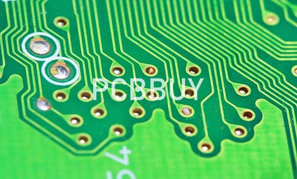
By stitching the traces on the different layers together with vias, you will effectively multiply the current carrying capacity from what it was on just a single layer. In the picture above, you can see a power trace on an internal layer of the board that has three stitching vias in it to connect with a companion trace on an adjacent layer. This can free up space for other routing or additional components on the external layers of the board.
The caveat is that you still have a great amount of heat that can be created in high current traces. By stitching multiple power traces together with vias on internal layers, you will provide a way for more metal to share the heat, but it will still need to be dissipated. This can be done with thermal vias that conduct the heat to metal landings on the external layers of the board for cooling. The more cooling you can provide for your high current traces, the better your board will operate and the less likely it will suffer thermal damage.
Industry Category


