What are the Main Types of Tests in PCB Manufacturing?
By:PCBBUY 08/28/2024 16:05
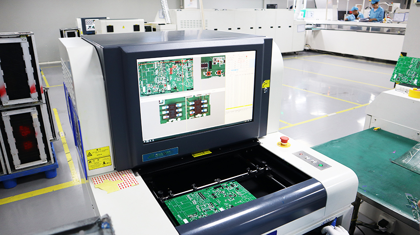
In the PCB manufacturing process, testing is very important. Conducting PCB tests during the production cycle helps save costs and avoid problems in the final production run. Although some design analysis techniques can be used in the early stages to reduce major issues in the manufacturing process, there are multiple testing methods for physical circuit boards. These tests, conducted on prototypes or small-scale components, focus on potential short circuits, solder joint problems, and functionality to ensure that each tested PCB works as expected.
Importance of PCB Testing
Testing is a crucial step in PCB manufacturing as it ensures that the board will perform its intended function without failure. The primary goals of PCB testing are:
1. Verification of Design: To ensure the PCB has been manufactured according to the design specifications.
2. Fault Detection: To identify any defects or errors that may have occurred during manufacturing.
3. Quality Assurance: To meet industry standards and customer requirements for performance and reliability.
4. Cost Efficiency: Detecting issues early in the manufacturing process to reduce the cost and effort of rework.
Overview of Common PCB Testing Methods
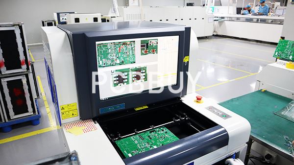
Several testing methods are employed at various stages of PCB manufacturing to ensure quality. These include:
Quality Assurance Testing
Electrical testing methods adopted by contract manufacturers (CMs) can be categorized by purpose. Tests used to measure circuit board connectivity fall under quality assurance or quality control, including:
What is Visual Inspection?
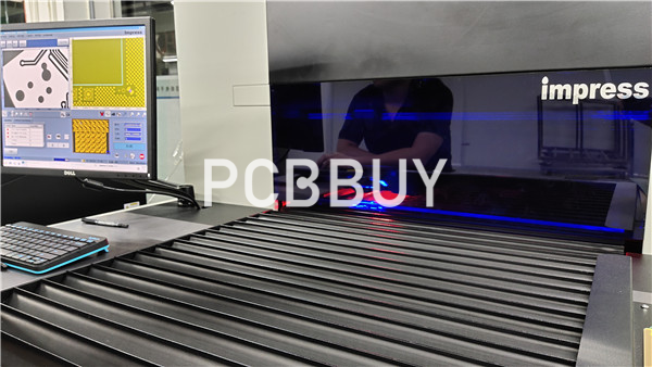
Visual inspection involves manually checking the PCB for any visible defects or abnormalities. This is typically the first line of defense in detecting obvious manufacturing defects such as misaligned components, solder bridges, or damaged traces.
Methodology
Manual Inspection: Human inspectors use magnifying glasses or microscopes to visually examine the PCB.
Automated Visual Inspection (AVI): Uses high-resolution cameras and image recognition software to identify defects.
Advantages and Disadvantages
Advantages:
- Simple and cost-effective.
- Useful for detecting large and obvious defects.
Disadvantages:
- Time-consuming.
- Not suitable for detecting microscopic defects or internal faults.
Automated Optical Inspection (AOI)
What is AOI?
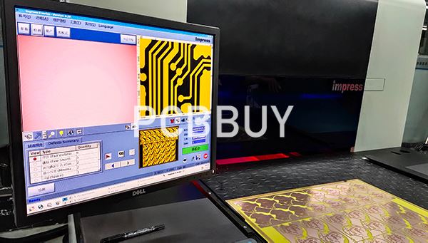
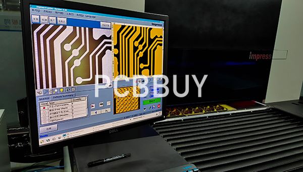
AOI is a non-contact testing method that uses optical cameras to capture images of the PCB. The images are then compared with a predefined template to detect any discrepancies.
Methodology
Image Capture: High-resolution cameras scan the PCB.
Data Analysis: Software compares the captured images with the reference design.
Fault Detection: Deviations are flagged for further investigation.
Advantages and Disadvantages
Advantages:
- High accuracy and speed.
- Capable of detecting a wide range of defects.
- Can inspect both assembled and bare PCBs.
Disadvantages:
- High initial setup cost.
- Limited to visual defects; cannot detect electrical or internal faults.
X-ray Inspection
What is X-ray Inspection?
X-ray inspection is used to detect hidden defects in PCBs, such as internal solder joint defects and misaligned components that are not visible to the naked eye or through optical inspection.
Methodology
X-ray Source: A beam of X-rays is directed at the PCB.
Image Capture: Sensors capture the X-ray image.
Data Analysis: The image is analyzed for defects.
Advantages and Disadvantages
Advantages:
- Can detect internal and hidden defects.
- Suitable for inspecting complex PCBs with multiple layers.
Disadvantages:
- Expensive equipment.
- Slower than other inspection methods.
Electrical Testing
Electrical testing is the most critical step in PCB testing as it ensures the board's functionality. Several electrical tests are performed, each targeting different aspects of the PCB's performance.
Flying Probe Testing
What is Flying Probe Testing?
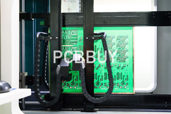
Flying probe testing uses movable probes to contact the PCB and perform tests without the need for a dedicated test fixture.
Methodology:
Probes Movement: Probes move across the PCB according to a predefined test program.
Contact Points: Probes touch the test points on the PCB to measure electrical characteristics.
Fault Detection: Any deviation from expected values is flagged.
Advantages:
- No need for a test fixture.
- Suitable for small production runs and prototypes.
- Quick and flexible setup.
Disadvantages:
- Slower than in-circuit testing for large volumes.
- Limited by the number of probes and their movement speed.
In-Circuit Testing (ICT)
What is ICT?
In-Circuit Testing involves using a bed of nails fixture to test the electrical performance of individual components on the PCB.
Methodology:
Fixture Setup: A custom fixture with multiple pins contacts the PCB at various test points.
Signal Application: Test signals are applied, and responses are measured.
Fault Detection: Identifies issues like shorts, opens, and incorrect component values.
Advantages:
- Comprehensive testing of the entire PCB.
- High speed and accuracy.
- Ideal for large production runs.
Disadvantages:
- High initial cost due to the need for custom fixtures.
- Not suitable for low-volume production.
Environmental Stress Testing
Environmental stress testing subjects the PCB to various environmental conditions to ensure its durability and reliability in real-world applications.
Temperature Cycling
What is Temperature Cycling?
Temperature cycling involves subjecting the PCB to alternating high and low temperatures to test its ability to withstand thermal stress.
Methodology:
Temperature Variation: The PCB is exposed to a range of temperatures.
Monitoring: The performance is monitored to identify any failures.
Advantages:
- Identifies potential failures due to thermal stress.
- Simulates real-world operating conditions.
Disadvantages:
- Time-consuming.
- Requires specialized equipment.

Humidity Testing
What is Humidity Testing?
Humidity testing exposes the PCB to high levels of humidity to test its ability to resist moisture ingress and corrosion.
Methodology:
Humidity Chamber: The PCB is placed in a chamber with controlled humidity levels.
Monitoring: The PCB is monitored for any signs of corrosion or failure.
Advantages:
- Ensures reliability in humid environments.
- Detects issues with material selection and manufacturing processes.
Disadvantages:
- Can be expensive and time-consuming.
- Not all failures will be detected immediately.
Industry Standards for PCB Testing
To ensure consistency and reliability, various industry standards govern PCB testing. Some of the widely recognized standards include:
IPC-A-600: Provides acceptance criteria for PCB manufacturing.
IPC-6012: Specifies the performance requirements for rigid PCBs.
J-STD-001: Sets the requirements for soldered electrical and electronic assemblies.
Conclusion
The testing of PCBs is a vital component of the manufacturing process, ensuring that the final product is reliable, meets design specifications, and can withstand the operational environment. By employing a combination of visual, optical, electrical, and environmental stress tests, manufacturers can effectively identify and rectify defects, thus ensuring high-quality PCBs that meet industry standards and customer expectations. As technology continues to evolve, so too will the methods and standards of PCB testing, keeping pace with the demands for increasingly sophisticated electronic devices.
Industry Category


