What are the Standards of PCB Gold Finger?
By:PCBBUY 07/29/2024 16:36
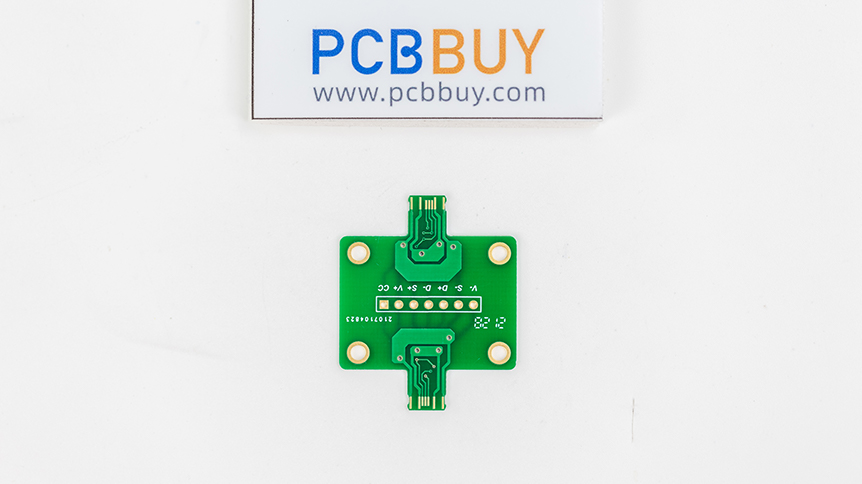
Gold fingers on printed circuit boards (PCBs) are vital connectors used for linking the PCBs to external components, such as peripheral devices or other circuit boards. These gold-plated contacts provide a reliable and durable interface, ensuring consistent electrical connectivity. This article delves into the standards governing PCB gold fingers, discussing their design, materials, PCB manufacturing processes, applications, and quality control measures, backed by professional knowledge and data.
Definition and Functionality
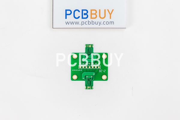
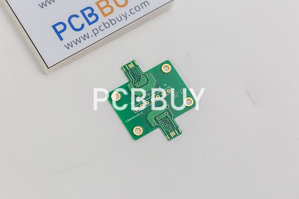
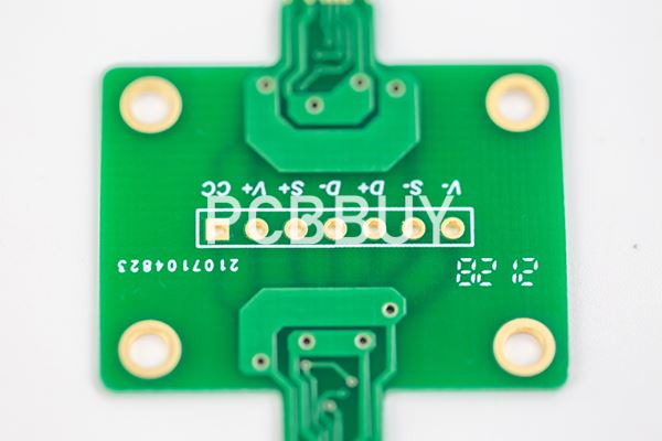
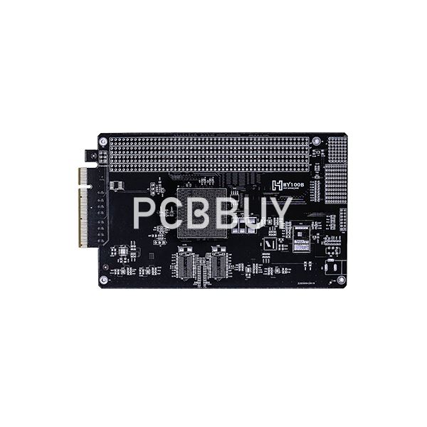
PCB gold fingers are the gold-plated connectors located along the edge of a PCB, commonly used in connectors like PCIe cards, memory modules, and other expansion cards. They serve as the contact points that interface with corresponding connectors in the devices they are plugged into, facilitating signal transmission and power distribution.
What Is the Importance in PCB Design?
The quality and durability of gold fingers are crucial for the overall performance and longevity of the device. Proper design and plating ensure low resistance and reliable contact, preventing data loss and ensuring smooth operation.
What Are the Materials Used in Gold Fingers?
Base Material: Copper
The base material for gold fingers is typically copper, selected for its excellent electrical conductivity. The copper layer is etched to form the finger pattern and then plated with nickel and gold to enhance durability and performance.
|
Material |
Electrical Conductivity |
Thermal Conductivity |
Role in PCB |
|
Copper |
High |
High |
Base layer for gold fingers |
Plating Layers: Nickel and Gold
The copper fingers are coated with a layer of nickel followed by a layer of gold. The nickel layer acts as a barrier, preventing the diffusion of copper into the gold layer, which could degrade the contact quality. The gold layer provides excellent conductivity, corrosion resistance, and durability.
|
Layer |
Thickness Range |
Purpose |
|
Nickel |
3-6 µm |
Barrier layer, prevents copper diffusion |
|
Gold |
0.5-1.27 µm (hard gold) |
Conductivity, corrosion resistance |
What Are the Types of Gold Used in PCB Gold Fingers
Hard Gold
Hard gold, also known as electrolytic gold, is commonly used for PCB gold fingers. It is an alloy of gold with other metals like cobalt or nickel, enhancing the wear resistance of the contact points. This type of gold plating is preferred for high-contact applications, such as connectors that will be frequently plugged and unplugged.
|
Type of Gold |
Composition |
Properties |
Typical Use |
|
Hard Gold |
Gold alloy with nickel or cobalt |
High wear resistance, durability |
Gold fingers, connectors |
Soft Gold
Soft gold, or pure gold, is used in applications requiring the highest conductivity and where the contacts will not be subject to significant mechanical wear. It is less common for gold fingers due to its lower durability compared to hard gold.
|
Type of Gold |
Composition |
Properties |
Typical Use |
|
Soft Gold |
Pure gold |
Excellent conductivity, low durability |
Sensitive electronic components |
What Are the Standards for PCB Gold Finger Design?
Dimensions and Tolerances
The dimensions of gold fingers, including their length, width, and spacing, must adhere to specific standards to ensure compatibility with connectors. These standards are often dictated by the type of connector being used and the industry requirements.
|
Parameter |
Standard Value/Range |
Description |
|
Finger Length |
Typically 1.0 - 2.0 mm |
Length of the contact area |
|
Finger Width |
Typically 0.5 - 1.0 mm |
Width of the contact area |
|
Finger Spacing |
Typically 0.5 - 1.0 mm |
Distance between adjacent fingers |
Plating Thickness
The thickness of the gold and nickel layers is critical for ensuring adequate durability and conductivity. Standards specify minimum and maximum thicknesses to balance cost and performance.
|
Layer |
Standard Thickness |
Purpose |
|
Nickel |
3-6 µm |
Barrier and support layer |
|
Gold |
0.5-1.27 µm (hard gold) |
Wear resistance, conductivity |
Edge Beveling
To facilitate smooth insertion into connectors, the edges of the PCB at the gold fingers are often beveled. This chamfering process reduces the risk of damage to both the PCB and the connector.
|
Feature |
Standard Angle |
Purpose |
|
Edge Beveling |
Typically 20-45 degrees |
Ease of insertion into connectors |
Manufacturing Process for PCB Gold Fingers
Patterning and Etching
The manufacturing process begins with patterning the copper layer on the PCB to form the finger outlines. This is typically done using a photolithographic process followed by chemical etching.
Nickel Plating
After the copper patterning, a layer of nickel is electroplated onto the gold finger areas. The nickel layer serves as a diffusion barrier and provides a robust base for the gold layer.
Gold Plating
Gold plating is applied over the nickel layer. The process involves immersing the PCB in a gold electrolyte solution and applying an electric current, which deposits a thin layer of gold onto the nickel surface.
Quality Control and Testing
The final step involves rigorous quality control to ensure that the gold fingers meet the required standards for thickness, adhesion, and electrical performance. This includes visual inspections, thickness measurements, and conductivity tests.
Quality Control Standards and Testing
Visual Inspection
Visual inspection checks for defects such as uneven plating, scratches, or contamination that could affect the performance of the gold fingers.
Thickness Measurement
Non-destructive testing methods like X-ray fluorescence (XRF) are used to measure the thickness of the nickel and gold layers. This ensures compliance with industry standards and specifications.
|
Test Method |
Purpose |
Standard Compliance |
|
X-ray Fluorescence (XRF) |
Thickness measurement |
Ensures plating meets required specifications |
Electrical Testing
Electrical tests verify the conductivity and resistance of the gold fingers. These tests ensure that the contacts will perform reliably in their intended applications.
Adhesion Testing
Adhesion tests evaluate the bond strength between the gold, nickel, and copper layers. Poor adhesion can lead to delamination and failure of the contact points.
What Are the Applications of PCB Gold Fingers?
Consumer Electronics
In consumer electronics, gold fingers are used in components such as memory modules, graphics cards, and expansion slots. Their reliability and durability are critical for ensuring consistent performance and user experience.
Industrial and Military Applications
In industrial and military applications, gold fingers are used in ruggedized connectors where environmental conditions can be extreme. The durability of gold plating is crucial for maintaining reliable connections in harsh conditions.
Telecommunications
In telecommunications, gold fingers are used in high-frequency connectors where signal integrity is paramount. The excellent conductivity and low contact resistance of gold fingers are essential for maintaining signal quality.
What Are the Challenges in Gold Finger Manufacturing?
Cost of Gold
Gold is an expensive material, and the cost of gold plating can be significant. Manufacturers must balance the thickness of the gold layer with performance requirements to optimize cost and functionality.
Environmental Concerns
The plating process involves chemicals and heavy metals, raising environmental and safety concerns. Compliance with environmental regulations and adoption of eco-friendly practices are important considerations.
Technical Limitations
Achieving uniform thickness and coverage in gold plating can be challenging, especially for complex designs. Advances in plating technology and process control are continually being developed to address these challenges.
What Are the Future Trends in Gold Finger Technology?
Advanced Plating Techniques
Innovations in plating techniques, such as pulse plating and selective plating, are being explored to improve the quality and efficiency of gold plating processes. These techniques can enhance the uniformity of the plating layer and reduce material consumption.
Nano-Coatings and Surface Treatments
Research into nano-coatings and advanced surface treatments aims to improve the performance of gold fingers. These treatments can enhance wear resistance, reduce contact resistance, and improve overall durability.
Miniaturization and High-Density Applications
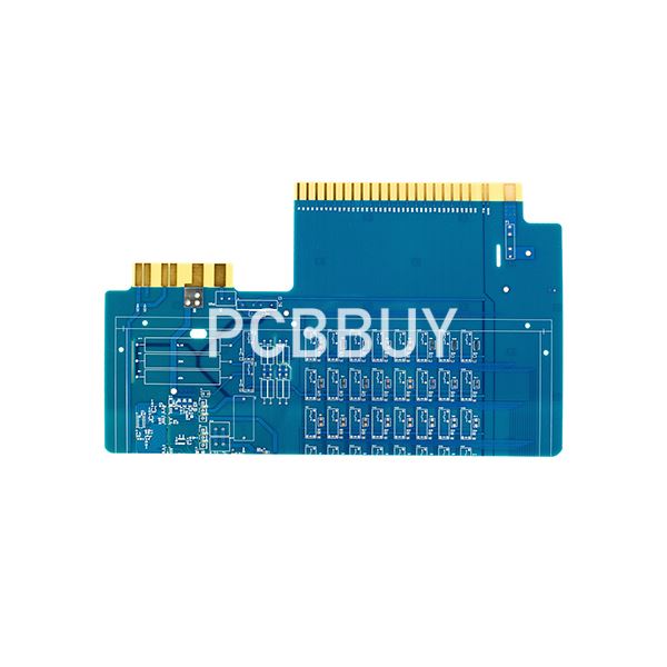
As electronics continue to miniaturize, the demand for high-density connectors with smaller and more closely spaced gold fingers is increasing. This trend challenges manufacturers to achieve precise patterning and plating at smaller scales.
Conclusion
PCB gold fingers are a critical component in a wide range of electronic devices, ensuring reliable electrical connectivity. Adherence to established standards for design, materials, and manufacturing processes is essential for achieving high-quality and durable connectors. While challenges such as cost and environmental concerns exist, ongoing advancements in materials and technology promise to enhance the performance and sustainability of gold fingers in the future.
References
1. IPC-4552, "Specification for Electroless Nickel/Immersion Gold (ENIG) Plating for Printed Circuit Boards," IPC, 2008.
2. A. Hall, "The Complete PCB Design Guide," McGraw-Hill Education, 2009.
3. J. H. Lau, "Advanced MEMS Packaging," McGraw-Hill Professional, 2010.
4. M. H. Azarian et al., "Reliability of Electronic Components and Systems," Springer, 2017.
5. K. C. Gupta et al., "Handbook of Flexible Electronics: Materials, Manufacturing, and Applications," Wiley, 2018.
Industry Category


