What are the career options for PCB students?
By:PCBBUY 12/25/2021 10:04

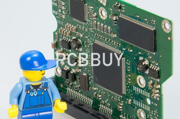
Printed circuit boards come in several flavors. The most common type is probably a two or four layer board that covers a few square inches. With today’s electronics, that’s actually quite a bit of space to fill. A junior designer may be called on to perform layout of adapters, interposers, extender cards and other basic layouts. There could be connectors and passive components but not necessarily any integrated circuits. If you find yourself doing the same board over and over again, it may be time to look for something else.
How to process the PCB career and what are the options for PCB student? How to become PCB industry practitioner? In this passage, please check and read the content below in this passage for more information.
What are the job contents of PCB career?
A PCB designer is responsible for taking a 2D schematic and creating the 3D CAD files used to manufacture the PCB. The first step is to create the component footprints, which show the size, shape, and orientation of each component. Second, the PCB designer creates a board outline with the dimensions and shape of the board as well as any keepout areas. Then the components with critical placement requirements are locked down, such as connectors that have to match up with another board.
Once this is complete, the rest of the parts are placed onto the board. Routing is the process of running traces between components to connect them together. Critical routing happens first, where traces that must be the exact same length or traces that must be a specific distance away from another trace are routed first. Then the rest of the board is routed, with traces going up and down through multiple layers of the board. The final task a PCB designer does is to generate all of the manufacturing files.
You can learn more about what PCB design is by reading our article.
A good PCB is part electrical engineer, part manufacturing expert, and part computer guru with a bit of process engineer thrown in the mix as well. Mostly though, a PCB has to have the ability to see beyond the lines and shapes of components on their computer screen in order to visualize where the design is headed. A good PCB fabrication can create something from nothing while solving many different puzzles along the way. For example, a rats nest is when the netlist is loaded and all the traces are run from component to component without any regard.

How to become a PCB designer for PCB students?
Education: Not only electronics but also basic physics and mathematics including geometry. Good communication skills are a must. There’s a bit of showmanship involved with managing expectations. A degree wasn’t always required. I managed to open some doors after six months in a trade school. Those high-school drop-out opportunities have faded away over time.
The pioneers: Names like Faraday, Henry, Ampere, Volta, Joule, Coulomb, Gauss and Ohm may be familiar. Also take the time to look up Gustav Kirchoff who built on Georg Ohm’s work. That leads to Maxwell’s equations and unlocks the foundation of electronics.
Getting the Job: Interviews can be tough. Preparation helps. To prepare for an interview with the Chrome book team at Google, I watched hours of videos about laptop repair. After a phone screen and a full day of on-site interviews, they still had more than one candidate. I was called in for a final exam with a duo of Managers. After the three rounds, they made me an offer that I couldn’t refuse.
The Kick-off: Somebody needs a board and you got the job. Expect a data dump and be ready to provide a time estimate. It seems prudent to sand-bag in case something goes awry. That’s a non-starter. They want a best-case scenario that you will adjust as you go. Set a few milestones to stay on course. If you want to stick around, you’ll execute the plan.
The Library: Any new components need to be accounted for. If your company has a librarian, you might be waiting for some footprints. Don’t let that prevent you from getting to the critical parts of the design. If you’re doing your own, make the most of it. A lot of the lingo is baked into the data sheets beyond the footprint diagram.
Place and Route: This is the main design work that starts with a board outline and a netlist that pulls in the library and the logic. Floorplanning is the first step. Determining the ideal stack-up is a close second. More often than not, these attributes will go through some iterations along the way.

How to process your education for PCB students?
Some engineers still perform the layout tasks themselves. If you are looking for a position that includes front end engineering and PCB layout, you will need to earn a BS degree in electronic engineering or a similar field. Many engineers go beyond a BS and pursue a master's degree.
Many companies are keeping engineers focused on the front end engineering side of product development and using PCB designers to focus on the layout side. There are some courses available for people looking to enter the PCB design market, including Fedevel and some community colleges. These are excellent ways to get a good starting point of an understanding of PCB design technologies and often offer a certificate of completion.
A widely accepted professional credential is fron the IPC (the Institute for Printed Circuits) which is a devopmental program focused on industry standards rather than company specific standards. Once a designer who has at least two years of experience has proven a complete understanding of current technologies and requirements, IPC provides either a CID or CID+ certification, which will certainly help you obtain your desired position.
Industry Category


