What are the types of IC packaging?
By:PCBBUY 06/30/2021 17:12

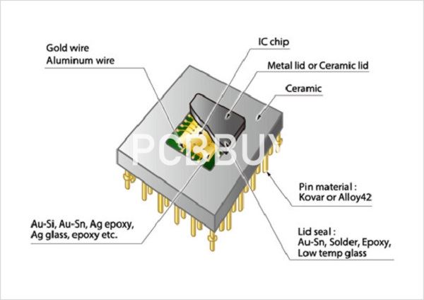
We’ll define IC packaging, also known as integrated circuit packaging, in simple terms. So, it refers to any component that has a semiconductor device. And the package is an encasement that surrounds the circuit device. Plus, its primary purpose is to prevent the device from: Physical impairment and Corrosion
It also serves as a platform that allows electrical contacts mounted on it to connect to the PCB. When it comes to IC packaging, there are different options to consider. And it’s because of the various circuits available. Also, these circuits have other requirements due to their outer shell.
In the passage, we are going to learn the types of IC packaging, please follow us and read the content we prepare for more information.
Why is IC packaging important?
The packaging of an integrated circuit is as important as the integrated circuit, the semiconductor device within. The packaging mainly serves three purposes – first, it protects the semiconductor circuit from physical impairment or damage. Secondly, it protects the circuit from corrosion. Finally and most important, it decides how electrical contacts are laid out from the semiconductor device over a PCB. This is an important consideration for both IC designing as well as PCB designing. Like how the connections are organized in an IC, how they are laid out using a standard IC package must be coherent with the application and various use cases of the respective IC.
What are the different types of IC packaging?
There are about ten different IC packaging types. But in this article, we’ll list four.
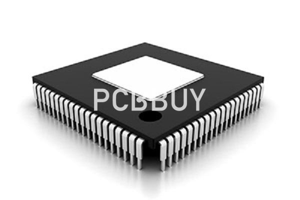
Through-Hole Mount Packages
This IC packaging is a mounting structure used for electronic parts. And they include the use of lead (Pb) on the parts that insert into the PCB’s drilled holes. They also get bonded to pads on the reverse side. And this happens by using mechanized insertion mount machines. Or by using manual assembly, which is hand placement. The Through-hole mount packaging is ideal for parts that aren’t suitable for surface mounting. An example of such is heatsinked power semiconductors and large transformers.
Surface Mount Packaging
The surface mount IC packaging refers to a method where electrical components are mounted directly on the PCB’s exterior. Any electric device that uses this method of IC packaging is a surface-mount device (SMD).
Also, the advent of the Surface mount packaging technology swallowed up the Through-hole mount packaging. Why was this so? It was because SMT supported increased automated manufacturing. And it enables quality improvement and cost reduction. But that’s not all. The surface-mount packaging has a platform that allows more components to get fitted to a specific area.
Also, when compared to through-hole mounts, SMT is smaller. And it’s because it has got smaller or no leads. Plus, it has the following:
· Flat contacts
· A lead of various styles or short pins
· Terminations on the component’s exterior
· A matrix of solder balls
Chip-Scale Packages
Another name for the Chip-Scale packages is chip-size packaging. It derived that name because it’s one of the few packages that come in chip size. For an IC package to be qualified as a chip-scale, it must meet these criteria:
· Be a single-die
· Have a direct surface mountable package
· Have an area that’s lesser than 1.2 times the size of a die
In 1993, Gen Murakami of Hitachi Cable and Junichi Kasai of Fujitsu proposed the above concept. However, Mitsubishi Electric created the first concept demo. The chip-scale technology requires the following:
First, the interposer where balls or pads get formed must hold the die. And this packaging is similar to the technology of the flip-chip ball grid array packaging. Second, the pads may be printed or etched directly into the silicon wafer. And this results in a packaging that almost has the size of the silicon die. A perfect example of such packaging is a water-level chip-scale package (WL-CSP) or a water-level package (WLP).
In the 1990s, the production of WL-CSP started. But a lot of companies began mass-producing it at the beginning of the 2000s. Advanced Semiconductor Engineering is an excellent example of a company that mass-produced the WL-CSP.

Ball Grid Array
Ball grid array is a type of packaging used to mount microprocessors permanently. But the package also provides more interconnection pins than a flat or dual in-line package. Hence, the best part of this package is:
You can use the entire bottom surface, not only the perimeter. And the traces joining to the package leads to the balls or wires. These balls or wires connect the die to averagely shorter packages, which are perimeter-only. In the end, the package brings about higher speed and better performance.
Also, as an engineer, you need precise control to solder BGA devices. And it’s because of its very delicate system. Thus, most companies stick to automated processes to avoid errors.
Industry Category


