BGA in PCB
By:PCBBUY 07/26/2021 09:17

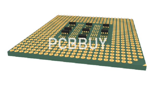
BGA packaging technology began to be applied in the 1990s. Now it is mainly applied to the packaging of high-end devices, with considerable development space. BGA is a kind of encapsulation technology in which many spherical convex points distributed in array form are soldered on the bottom or upper surface of the module. Among all the packaging typed of semiconductor IC.
In this passage, we will provide you everything about BGA in PCB, please follow us and read the content we prepare.
What are the classifications of BGA in PCB?
There are many types of BGA packaging, the general shape structure is square or rectangular. According to the arrangement mode of solder ball welding, it can be divided into peripheral type, staggered type and full array type BGA. According to the different substrates, it can be divided into 3 types as following:
PBGA (Plastic Ball Grid Array)
CBGA (Ceramics Ball Grid Array)
TBGA (Tape Ball Grid Array)
PBGA
Some PBGA are encapsulated as cavity structures, which are divided into 2 types: cavity up and cavity down. This kind of PBGA with cavity is designed to enhance its heat dissipation performance, which is called thermal enhanced BGA, or EBGA, or CBGA (Cavity Plastic Welding Ball Array).
The advantages of PBGA packaging are as follows:
· Good thermal match with PCB board.
· During reflow soldering, the self-aligning of the solder ball, that is, the surface tension of the solder ball, can be used to achieve the alignment requirements between the solder ball and the pad.
· Low cost.
· Good electrical performance.

CBGA
CBGA has the longest history in the BGA packaging series. Its base substrate is multilayer ceramics. The metal cover board is welded on the base substrate with sealed solder to protect the chip, lead and pad. The welding ball material between the solder ball and the package body needs to use cryogenic eutectic solder 63Sn37Pb.
The advantages of CBGA packaging are as follows:
· Good air tightness, high humidity resistance, and high long-term reliability of packaging components.
· Better electrical insulation performance than PBGA devices.
· Higher packaging density than PBGA devices.
· Better heat dissipation than PBGA devices.
TBGA
TBGA is a cavity structure. There are two ways of interconnection between the chip and substrate encapsulated by TBGA: inverted solder bonding and lead bonding. The chip is connected in the flexible multi-layer wiring belt. The circumferential array solder ball used as circuit I/O end is installed under the flexible carrier belt. Its thick sealing cover board is a radiator (heat sink), and also plays the role of strengthening the encapsulation body, so that the solder ball under the flexible substrate has better coplanability. Chip bonding on the copper heat sink of the core cavity. The bonding leads of the chip bonding pad and the multi-layer flexible wiring ad are used to realize interconnection. The circuit chip, lead, and flexible load pad are encapsulated with a sealant.
The advantages of TBGA are as follows:
· The flexible loading belt of the packaging body and the thermal matching performance of PCB board are good.
· During reflow soldering, the self-aligning of the solder ball and the surface tension of the solder ball can be used to achieve the alignment requirements between the solder ball and the pad.
· Is the most economical BGA packaging.
· Better heat dissipation performance than PBGA structure.
What are the features of BGA?
· More I/O. Since BGA encapsulated solder balls are arranged under the encapsulated substrate in the form of array, the number of I/O of the device is greatly increased, the size of the encapsulation body is reduced, and the space od assembly is saved.
· High packaging yield reduces cost.
· The contact surface between BGA’s array welding ball and substrate is large and short, which is conducive heat dissipation.
· The pin of BGA array welding ball is short, which shortens the signal transmission path, reduces the lead inductance, electrical resistance and improves the circuit performance.
· Improve the coplanability of I/O terminal and reduce the loss caused by poor coplanability in the assembly process.
· BGA is suitable for MCM encapsulation and can achieve high density and high performance of MCM.
· The IC of BGA and fpBGA is stronger and more reliable than the foot-shaped package of detail spacing.
Industry Category


