BGA soldering
By:PCBBUY 08/04/2021 08:58

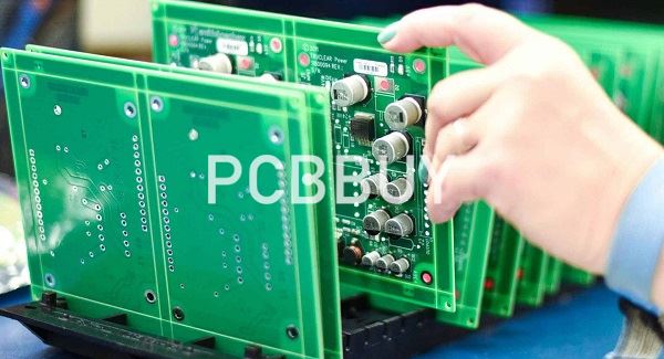
More electronics components with fine-pitch IC packaging have been assembled on PCB, especially BGA (ball grid array) and CSP (chip-scale package) components. There are lots of challenges of BGA soldering. In this passage, we will focus on the topic and you could check the content we provide for more information.

What are the reasons of BGA soldering defects?
Incorrectly-Picked Tg and Td of PCB Substrate Material
During the process from lead manufacturing to lead-free manufacturing, reflow soldering and wave soldering temperature has to rise up due to SMT (surface mount technology) assembly requirement. Some people simply believe it OK that substrate material with high Tg (glass transition temperature) is selected for PCB board. They just think that it's essential to manage and control Z-axis expansion. The primary aim is to stop delamination from taking place of thick circuit boards and 14-layer or more PCBs and to stop cracks from occurring to PTH (plated through hole) because a large extent of Z-axis expansion of PCB tends to lead PTH hole wall to break during reflow or wave soldering. Nevertheless, Tg fails to defeat cracks generated during lead free process unless Td (temperature of de-composition) is considered to totally solve PCB cracks issue. Three levels of Td are regulated in IPC concerning PCB substrate material: 310°C, 325°C and 340°C.
In conclusion, during the process of substrate material determination, the higher Tg and Td are, the better. But PCB fabrication cost is an essential consideration based on which substrate material with agreeable Tg and Td should be picked up.
Insufficient Gel Content in Prepreg
Insufficient gel content in prepreg used on external layers and between internal layers tends to lead copper foil to generate bubbles under high temperature.

Unsuitable Copper Profile Selection
Generally, ordinary profile is classified into three categories: standard profile, lower profile and very lower profile. Standard profiles contain no regulations on copper sheet because adhesiveness is high but too high profile tends to cause bad etching, which further reduces stability of line width and impedance control. Lower profile regulates that maximum Profile SPEC is 0.4mil (10.2μm). Up to now, lower profile has been leveraged by most PCB manufacturers. Very lower profile regulates that maximum Profile SPEC is 0.2mil (5.1μm), which is generally only leveraged in multilayer PCB fabrication with special fine line requirement such as 2mil trace width.
Low-Performed PCB Lamination
Whenever low-performed PCB lamination takes place, insufficient melanism or brownization will lead to bad adhesiveness.
Low-Performed Solder Mask Developing or Surface Finish
Low-performed solder mask developing or surface finish will cause soldering defects. For example, surface oxidation tends to be generated when OSP film is too thick or too thin, receives unsuitable pre-process or goes through too long holding time.
Too Small BGA Pad Size
During the design phase, when BGA pad size is too small, it takes place possibly due to over etching or absence of compensation value of etching factor.
Insufficient Process Control
• During stencil design phase, four corners and each side of BGA component should be 1mil to 2mil larger than those of pad. Stencil opening size should be designed based on specs of BGA components including pitch, soldering balls on BGA and ingredient of soldering balls.
• During the process of printing, support pin shouldn't be against BGA to stop fake soldering and pillow effect from taking place due to contamination of BGA pad. Furthermore, especially much attention has to be paid to printing scraper pressure and printing quality control.
• Wafer positions of pickup BGA, component thickness setting and pressure amount of pickup should be emphasized during mounting stage.
• There are more opportunities for cracks during IR reflow and special attention has to be paid:
a. During the process of double-side PCB fabrication, PCB deformation degree has to be considered. Fixtures can be used during reflow soldering and substrate of fixtures has to be carefully considered for its possible shrinking due to high temperature and cooling.
b. Incoming BGA components have to be carefully inspected to see whether sinking does take place on soldering balls. Moreover, alloy ingredient of soldering balls and compatibility between Z-axis expansion of substrate material of BGA and PCB board.
Industry Category


