What is Design for Testability (DFT) in PCB Manufacturing?
By:PCBBUY 06/27/2024 16:12
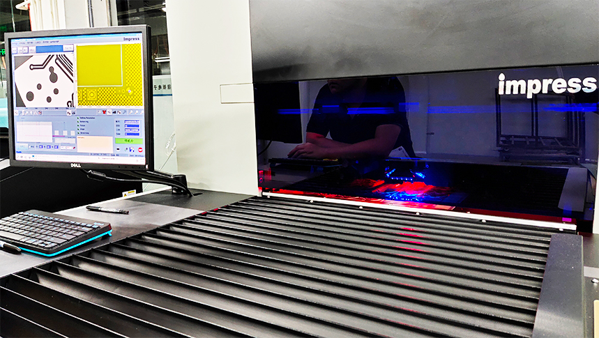
In the process of PCB production and manufacturing, one indispensable part is to test the assembled PCBs for functionality and manufacturability. This professional term, Design for Testability (DFT), involves a series of checks performed after reflow soldering, wave soldering, or a combination of both, such as X-ray, AOI, ICT, and FCT inspections.
Unlike Design for Manufacturability (DFM), which identifies and solves potential issues before manufacturing, DFT checks and resolves problems during the production process. Both DFM and DFT are equally crucial. In more technical terms, PCB Design for Testability (DFT) is a method for optimizing circuits and layouts for operational and functional tests. DFT can identify short circuits, open circuits, component placement errors, or faulty components.
DFT primarily verifies the following three issues:
1. Is the circuit board design accurate?
2. Is the circuit board production flawless? Are there any defects?
3. Are all components, chips, and connections on the PCB functioning properly?
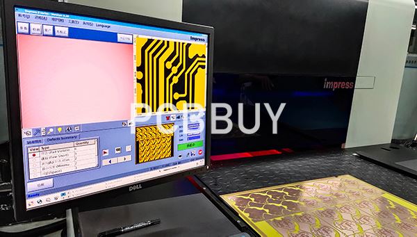
Additional issues to be addressed include:
1. Proper spacing of components to reduce the risk of test defects.
2. Ensuring correct solder mask between pads to maintain electrical performance.
3. Optimizing drill bit sizes.
4. Addressing improper surface mount pad sizes.
5. Acid trap detection.
Parameters Included in PCB DFT
1. Test Points
Test point insertion is essential in DFT to improve test efficiency. The position of test points depends on the number of components they can cover. Accurate power and ground test points help mitigate signal integrity issues.
2. Test Traces
You can place test points on traces sensitive to analog signals, connecting them to oscilloscopes or signal generators to understand signal behavior.
3. LEDs
Adding LEDs helps determine whether the power is on or off. Debug LEDs are suitable for FPGAs or microcontrollers and are useful in mass production.
4. Headers
Test points connected to vias for voltage measurement.
Technologies Involved in PCB DFT
1. PCB Bare Board Testing
Bare board tests are performed before assembling components to check PCB connectivity. Methods include isolation tests (verifying resistance between two electrical connections) and continuity tests (checking for open circuits).

2. PCB Assembled Board Testing
Post-assembly tests ensure the integrity and functionality of the circuit board.
Seven PCB Testing Techniques
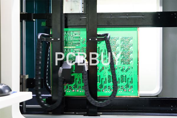
1. Flying Probe Testing
Suitable for both bare and assembled boards, flying probe testing uses needles to check passive components, open circuits, short circuits, measure voltages, and verify diode and transistor placements.
Advantages:
- Cost-effective.
- Higher test coverage.
- No fixtures required.
- Quick implementation.
Disadvantages:
- Time-consuming due to probe movement.
- Difficult to set up without test points or test vias.
- Limited to testing only parallel capacitors.
2. ICT Testing
In-circuit testing (ICT) uses pre-installed electronic probes aligned with access points on the PCB to establish stable electrical connections. ICT checks for short circuits, open circuits, solder mask defects, and component misplacement.
Advantages:
- Suitable for mass production.
- Up to 90% coverage.
- Reduces human error.
Disadvantages:
- Not ideal for small batch production.
- Cannot detect voids or insufficient solder masks.
- Expensive.
3. FCT Testing
Functional circuit testing (FCT) ensures quality control and verifies the expected operation of the device. It involves basic switch tests and may require complex software and protocols to test the PCB under real-world conditions.

Advantages:
- Low cost.
- Versatile and customizable.
- Does not affect PCB lifespan.
Disadvantages:
- Requires experienced technicians.
4. AOI Testing
Automated Optical Inspection (AOI) uses 2D or 3D cameras to capture high-resolution images and verify the schematic against a database. AOI can accurately detect all visible errors and is often used alongside other testing methods like flying probe or in-circuit testing.
Advantages:
- Detects critical defects accurately.
- Consistent method.
Disadvantages:
- Only detects surface defects.
- Time-consuming and requires setup changes based on design.
5. Burn-in Testing
Burn-in testing subjects the PCB to conditions beyond specified operational limits to trigger potential failures, determining the maximum operating ratings of the PCB.

Advantages:
- Enhances product reliability.
- Verifies functionality under environmental conditions.
Disadvantages:
- Can shorten PCB lifespan.
- Requires significant time and effort.
6. X-ray Testing
X-ray inspection detects hidden components, solder joints, BGA packages, internal traces, and barrel defects.
Advantages:
- Non-destructive inspection.
- Can examine internal layers.
Disadvantages:
- Requires skilled technicians.
- Labor-intensive and costly.
7. Manual Visual Inspection
Technicians inspect the PCB visually or with magnifiers to identify component alignment issues, missing components, and other defects.
Advantages:
- Simple and basic method.
Disadvantages:
- Prone to human error.
- Cannot detect tiny or invisible defects.
Comprehensive Guide to PCB Inspection Techniques and Applications
Printed Circuit Boards (PCBs) are the backbone of modern electronic devices, ensuring the proper electrical connections between components. The reliability and performance of electronic products significantly depend on the quality of the PCBs used. Therefore, various inspection techniques are employed during the manufacturing process to ensure PCB quality and functionality. This article explores three major PCB inspection techniques: Visual Magnification Inspection, Metallographic Cross-Section Analysis, and Microscopic Morphology Inspection. Each section will detail the principles, applications, and importance of these techniques, supported by data and tables for clarity.
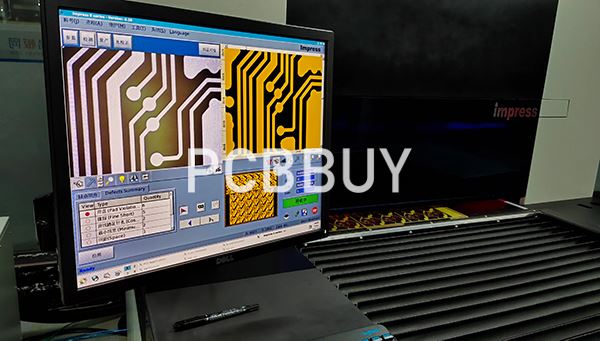
Visual Magnification Inspection Techniques and Applications
Visual Magnification
Inspection involves the use of magnification tools, such as microscopes and magnifiers, to examine the surface of the PCB for defects. This technique is crucial for detecting visible flaws that may affect the board's performance and reliability.
Principles and Tools
Microscopes: Microscopes with various magnification levels (typically 10x to 100x) are used to inspect fine details on the PCB surface, including solder joints, traces, and components.
Magnifiers: Handheld or stand-mounted magnifiers provide a more portable solution for inspecting larger areas of the PCB.
Applications
Visual Magnification Inspection is used to detect:
Solder Joint Defects: Poor solder joints can lead to intermittent or failed connections. This technique helps identify issues such as cold solder joints, solder bridges, and insufficient solder.
Trace Defects: Breaks, nicks, or thinning in copper traces can be detected, which might otherwise lead to circuit failure.
Component Placement: Ensuring that components are correctly placed and oriented according to the design specifications.
Data and Analysis
|
Defect Type |
Detection Rate |
Magnification Level |
|
Magnification Level |
95% |
20x - 50x |
|
Trace Defects |
90% |
10x - 30x |
|
Component Placement |
85% |
10x - 20x |
Advantages and Limitations
Advantages:
- Cost-effective
- Non-destructive
- Immediate feedback
Limitations:
- Subjective results (depends on the inspector's skill)
- Limited to surface defects

Metallographic Cross-Section Analysis Techniques and Applications
Metallographic Cross-Section Analysis involves slicing a PCB sample to examine its internal structure. This technique provides detailed insights into the PCB's layer composition, solder joints, and via structures.
Principles and Tools
Sectioning: A small section of the PCB is cut out using precision saws.
Mounting: The section is mounted in a resin for stability.
Grinding and Polishing: The mounted sample is ground and polished to a smooth finish.
Etching: Chemical etching is used to highlight different materials.
Microscopic Examination: The sample is examined under a microscope, typically with magnifications of 100x to 1000x.
Applications
Metallographic Cross-Section Analysis is used to:
Inspect Solder Joints: Evaluate the quality and reliability of solder joints.
Analyze Vias and PTHs: Check the integrity of plated through-holes (PTHs) and vias.
Layer Structure Analysis: Examine the number and quality of PCB layers.
Data and Analysis
|
Parameter |
Typical Values |
Magnification Level |
|
Solder Joint Thickness |
20-50 microns |
200x - 500x |
|
Copper Layer Thickness |
18-35 microns |
100x - 200x |
|
Via Diameter |
0.2-0.5 mm |
100x - 300x |
Advantages and Limitations
Advantages:
- Detailed internal structure analysis
- High accuracy
- Identifies hidden defects
Limitations:
- Destructive testing
- Time-consuming
- Requires specialized equipment and expertise
Microscopic Morphology Inspection Techniques and Applications
Microscopic Morphology Inspection focuses on examining the surface and subsurface features of the PCB at a microscopic level. This technique is essential for detecting micro-level defects that can affect the PCB's performance.
Principles and Tools
Scanning Electron Microscopy (SEM): Provides high-resolution images of the PCB surface and subsurface, allowing for detailed defect analysis.
Atomic Force Microscopy (AFM): Measures surface roughness and topology with nanometer resolution.
Optical Microscopy: Uses visible light and high magnification lenses to inspect fine details on the PCB surface.
Applications
Microscopic Morphology Inspection is used to detect:
Surface Roughness: Ensures that the PCB surface meets the required specifications for component mounting.
Micro-cracks: Identifies tiny cracks in solder joints and traces that may lead to failure.
Contaminants: Detects contamination that could affect the PCB's performance.
Data and Analysis
|
Defect Type |
Detection Rate |
Magnification Level |
|
Surface Roughness |
98% |
500x - 1000x |
|
Micro-cracks |
95% |
1000x - 5000x |
|
Contaminants |
90% |
200x - 1000x |
Advantages and Limitations
Advantages:
- High resolution and precision
- Can detect very small defects
- Non-destructive (for SEM and AFM)
Limitations:
- Expensive equipment
- Requires skilled operators
- Time-consuming analysis
PCB inspection is a critical step in ensuring the reliability and performance of electronic devices. Visual Magnification Inspection, Metallographic Cross-Section Analysis, and Microscopic Morphology Inspection each play unique roles in identifying defects at different stages of the PCB manufacturing process. By employing these techniques, manufacturers can ensure high-quality PCBs, reduce the risk of failures, and improve overall product reliability.
References
He Wei, PCB Basic Electrical Information Science and Technology, China Machine Press,432-437
Industry Category


