What is ENEPIG Finish in PCB Manufacturing Process for Beginners?
By:PCBBUY 10/22/2021 09:33

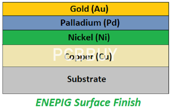
ENEPIG is a kind of selective surface processing technology, is also a kind of new surface treatment technology, the principle for the PCB copper layer on the surface of the plating layer of nickel, palladium and gold, the main process includes:
Do you want to know ENEPIG finish in PCB? Do you want to learn more information about ENEPIG finish in PCB? Please check and read the content below for more professional knowledge.
What are the features of ENEPIG finish in PCB?
· For wire bonding applications, the pull strength is of high importance. ENEPIG offers a greater pull strength (aluminum wire: up to 10 gram-force; gold wire: up to 8 gram-force) than soft gold and ENIG (Electroless Nickel Immersion Gold). Hence, becomes the right choice.
· The multiple electroless deposition of nickel, palladium and gold metals help minimize porosity and protects the cupper layer beneath them.
· While dealing with high-frequency circuits, nickel might interfere and retard high-frequency signals. With the palladium layer on top of nickel, it can negate the influence of nickel on high-frequency signals.
· In mixed technology i.e. when RF and digital circuits are involved, opting for direct gold surface finish will lead to assembly related issues. Whereas, ENEPIG is compatible with mixed technology and the various assembly processes.
· ENEPIG surface finish is the low-cost alternative to direct soft gold plating.
ENEPIG surface finish is ideal for soldering, aluminum wire bonding, and gold wire bonding. This surface finish is formed by the sequential deposition of nickel, followed by palladium, followed by immersion gold. The Nickel acts as a barrier layer and reduces copper dissolution during wave solder, and ensures fine solderability. Nickel also prevents the mixing of copper and solder.
What are the advantages of ENEPIG finish in PCB?
Nickel electroplating through the electroplating method, the gold particles are attached to the PCB board. It is also known as hard gold because the adhesion is strong. Using this process can greatly increase the hardness and wear resistance of the PCB. Also, it can effectively prevent copper and other Metal diffusion, and meet the requirements of hot compression welding and brazing.
Immersion gold is a chemical reaction that causes gold particles to crystallize and attach to the PCB pads. Because of its weak adhesion, it is also called soft gold.
In the PCB prototype process, ENEPIG, nickel electroplated gold and immersion gold all belong to the surface treatment process. The difference is that nickel electroplated nickel is done before the solder mask while ENEPIG and immersion gold are done after the solder mask.

What is the work principle of ENEPIG finish in PCB?
ENEPIG involves four layers of metal deposited on a PCB surface. These are copper, nickel, palladium and gold. The process of creating an ENEPIG surface finish includes the following steps:
Copper Activation
In this step, the copper layer that needs protection is selectively activated, which determines the deposition pattern in the electroless nickel plating step. This process is accomplished using a displacement reaction, which makes the copper layer act as a catalytic surface.
Electroless Nickel
Nickel acts as a barrier layer, preventing copper from interacting with the other metals involved in this plating technology, particularly gold. The layer is deposited on the catalytic copper surface using an oxidation-reduction reaction. The result is a layer that is between 3.0 to 5.0 microns thick.
Electroless Palladium
The layer of palladium is what differentiates ENEPIG from ENEG surface finish technology, acting as another barrier layer. Palladium prevents the nickel layer from corroding and diffusing into the gold layer. It also acts as an anti-oxidation and anti-corrosion layer. Like nickel, this layer is deposited using an electroless reaction, which uses a chemical oxidation-reduction reaction to cause the nickel surface to react with palladium and form a thin layer. This palladium is deposited on a layer with a thickness of 0.05 to 0.1 microns, depending on the application.
Immersion Gold
Gold is the final layer added to ENEPIG surfaces, lending the benefits of low contact resistance, protection from friction and resistance to oxidation. Gold also preserves palladium’s solderability. As the name suggests, immersion gold plating services completely immerse the covered PCB, using a displacement reaction where palladium on the PCB dissolves and releases electrons that reduce the gold atoms surrounding it. The gold ions then attach to the surface of the PCB, replacing some palladium ions and resulting in a relatively thin outer layer, between 0.03 and 0.05 microns thick — substantially lower than any other solution using gold plating techniques.

Why PCBBUY is professional at ENEPIG?
This process is not common because the nickel palladium has certain requirements on the process capacity of the plate plant, so many enterprises cannot find a suitable plate plant.
At present, PCBBUY has been fully online nickel palladium process, to solve the problem of enterprises. PCBBUY also supports a variety of complex processes, such as custom laminated structures, ultra thin sheets, large size boards, etc. As a professional PCB manufacturer of 1-8 layers, PCBBUY will continue to solve the problems of various precision boards and difficult boards for customers.
Industry Category


