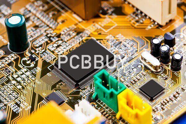
ENIG finish PCB
By:PCBBUY 06/02/2021 17:45

ENIG (Electroless Nickel Immersion Gold) is surface plating that is applied over the copper pads on a Printed Circuit Board to protect them from corrosion and other abnormalities. Initially, the copper pad is covered by a Nickel (Ni) layer followed by a thin immersion Gold (Au) layer. ENIG provides good oxidation resistance, excellent surface planarity and allows for easy soldering which results in excellent electrical performance of the PCB board.
When the surface finish is processing, there are metal or organic material optional. The surface finish you choose for your PCB will have a significant impact on its quality and usefulness within its parent part. The finish prevents the PCB’s copper layer from oxidizing, which would otherwise decrease its solder ability. Applying a finish protects the board from oxidizing before the components are added, ensuring that you can solder the additional elements as needed. Because the PCB’s electrical connections rely on adequate copper conductivity, it’s essential to prevent oxidation and adhere the components as necessary.
And among several types of surface finishing, we are going to talk about ENIG. Check the content we provide below for more information.
What is ENIG?
Despite the higher pricing of ENIG surface finishing, it has a high success rate for producing high-quality PCB products. It holds up under multiple thermal cycles, showcases great solderability and is a suitable option for wire bonding. As the name suggests, it consists of two coating layers — nickel and gold. The nickel protects the base copper layer and enables secure attachment of electrical components, while the gold serves as an anti-corrosion measure for the nickel.
ENIG can be used in situations where tight tolerances are required for PCB elements like plated holes, as HASL is not as effective for this. Like OSP, it offers excellent flatness and is ideal for fine pitch devices.
Applying the ENIG coating requires nickel to be deposited onto a copper surface catalyzed with palladium. The immersion gold stage causes the gold to adhere to the nickel by way of a molecular exchange. ENIG is similar to OSP in its inclusion of micro-etching and rinsing between each stage — the process includes these steps:
-Cleaning.
-Micro-etching.
-Pre-dipping.
-Applying the activator.
-Post-dipping.
-Applying the electroless nickel.
-Applying the immersion gold.
-Standard applications for an ENIG surface finish include:
Complex surface components: Because of its flat surface, this finish type is a preferable choice for complex PCB components requiring smooth surfaces, like ball grid arrays (BGAs) or quad flat packages (QFPs).
Wire bonding: ENIG finishes allow for minimal wire bonding for aluminum wires, although they are not compatible with gold.
High reliability applications: You will often find ENIG surface finishes used for PCBs in industries such as aerospace, military, medical and high-end consumers. Its quality makes it suitable for applications where precision and durability are vital.
What is ENIG black pad?
There might not be any topic more controversial in the PCB industry than that of ENIG black pad. In simple terms, black pad refers to an inferior connection that occurs between the solder and nickel interface. While many professionals consider this phenomenon to be extremely rare — occurring by some estimates in less than one or two percent of ENIG PCBs — the fact that a black pad problem isn’t typically discovered until an assembly process commences makes it a costly error to discover and correct in the post-manufacture phase.
Black pad is the result of the immersion gold and electroless nickel process. While it produces a highly solderable finish — ideal for applications where reliability and complex circuitry go hand-in-hand — the process can also create flawed joints that, when stressed, will break their connections. The resulting open circuits expose a layer of dark nickel that’s corroded — which gives this phenomenon its notable name “black pad.”

According to recent research and industry reports, black pad is the result of an excessive level of phosphorous that’s a byproduct of the dissolution of nickel. Ultimately, as the result of consecutive reflow processes, a starting seven percent phosphorous level can easily climb to nine percent — or even higher. And the higher the level of phosphorous, the greater the risk of nickel corrosion is during the gold immersion/deposition process.
What are the advantages of ENIG?
-Flat surface, good for small SMD devices,
-Reworking availability (>3 times reflow),
-Excellent electrical conductivity,
-Anti-oxidation & anti-rust,
-Good heat dissipation,
-Higher surface thickness
Industry Category


