What is Edge Connector Beveling in PCB Manufacturing?
By:PCBBUY 01/20/2022 09:16

Edge connector beveling is the cutting or shaping of an edge connector at an angle or slant. Any beveled connector PCB or other makes the entry of the board into the connector easier. Edge connector beveling is a parameter in the order details that you have to select and check when this option is required.
In this passage, we are providing all the information of edge connector beveling in PCB. If you are searching for the professional knowledge of edge connector beveling in PCB, please check and read the content below.
Why edge connector beveling in PCB is necessary?
PCBs’ connection points are primarily subjected to constant unplugging and plugging based on the nature or role of interconnecting PCBs. Therefore, if there is no durable contact edge, then this means that they are prone or subject to wear-and-tear that may bring about device malfunction.
The habit of using gold to plate a majority of connectors helps prolong the durability of edge connectors. But isn’t gold too expensive of all the metals out there? Other metals such as copper can work fine, but gold is preferred based on plenty of advantages that it offers.
Gold has always been preferred over other metals since it has proven to be highly corrosive resistant and consists of high electrical conductivity. Better yet, gold can be easily alloyed with nickel or cobalt to increase further its ability to withstand wear and tear after a short time.
There have been earlier experiments undertaken to find out the resistance of gold compared to other metals, and gold has shown to consist of one of the lowest resistance levels compared to other metals. Better yet, gold has also been found to be highly inert and does not oxidize or immediately react with other metals.

What are chamfering of edge connector beveling in PCB?
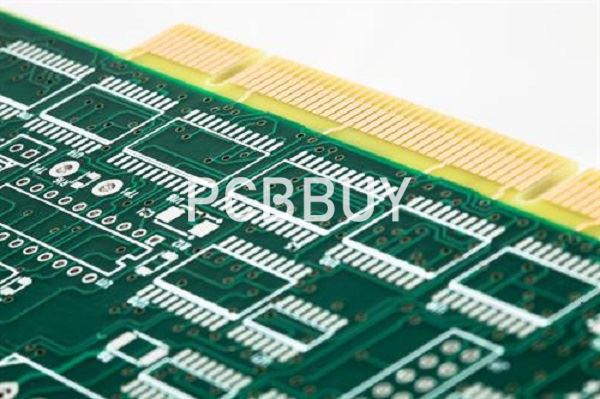
An edge connector is a female connector that mates with the contact pads lining the edge of a PCB. Think of those PCI and PCI slots that make it easy to add memory cards into the motherboard of your PC. When a product supports hardware upgrades, edge connectors are often the standardized interface of choice.
As the designer, it’s your job to make sure your board can easily mate with the standard edge connector on the mating board. That’s where chamfering comes in—you need to ensure that the mating edge of your PCB meets the chamfer angle and tolerances specified by the edge connector manufacturer. You’ll also want to make sure the fabrication house you choose is capable of meeting the tolerances and chamfer angle you desire. To give you an idea, here are some common design parameters you’ll encounter for PC and PCI cards:
· Chamfer angle: 45° for PC, 20° for PCI
· Chamfer depth: 0.5 mm for PC and PCI
· Gold finger spacing: 0.7mm for PC, 2.0mm for PCI
What are the limitations of edge connector beveling in PCB?
Gold finger technology is of great importance. But sadly, its application remains limited due to several reasons. For instance, plated pads have to be on the edge of the PCB. Since gold plating requires an electroplating process, there has to be a connection that links the plated pads and the panel frame.

Most plating pads manufactured by players in the industry produce fingers that do not exceed over 40mm. If you require longer or oversized gold fingers, then the process of creating them will intensify.
The above is not all. If you don’t know, the inner layers of the edge connectors must be free of copper material. Otherwise, the entire process/steps of beveling the contacts can expose the copper material.
Apart from flexible printed circuit boards, when gold-plating on both sides of the PCB, the least separating distance between the lower and the upper layers of the printed circuit board is supposed not to exceed 150mm, while the maximum length should not be more than 40mm.
There are other rare cases where gold fingers appear shorter or longer than the rest. It means that the shorter pads will not fail to be connected vertically to the plating bar, an aspect that may go ahead to affect matters to do with functionality.
Industry Category


