What is Edge Plating in PCB with 7 Common Factors for beginner?
By:PCBBUY 11/06/2021 10:26

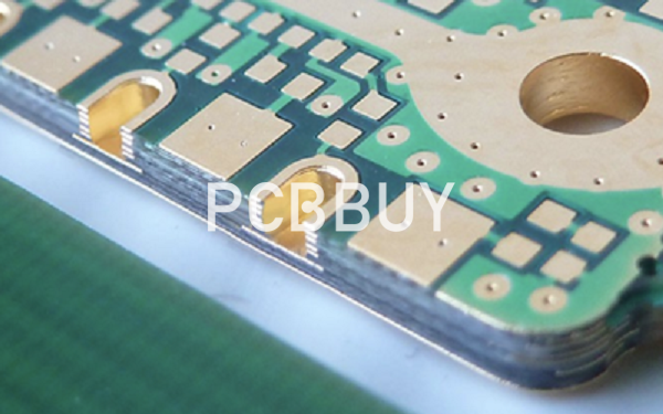
As you know, there are a great deal of challenges for a PCB manufacturer mainly in how to prepare the plated edges and the life span adhesion of the plated material, what’s more, it needs the precision handling in PCB manufacturing that is used for edge PCB soldering. PCBGOGO can make sure that the PCB edge castellation thoroughly prepares edges surfaces, which applies the plated copper for prompt adhesion and processes the circuit board to make sure the long-term adhesion between each layer.
If you are going to learn more about edge plating in PCB, please check and read the content for more professional information.
1. What are the applications of edge plating in PCB?
Edge plating circuit boards are common in many industries, and edge plating is a common practice. You’ll find PCB edge castellation (or edge plating PCBs) applied in many cases, including:
· Improving current-carrying capabilities
· Edge connections and protection
· Edge soldering to improve fabrication
· Better support for connections such as boards that slide into metal casings
2. What are the advantages of edge plating in PCB?
But there are more benefits to the performance of your printed board when it’s edge plating.
· Thermal Distribution: One of the key benefits of edge plating is its ability to support thermal distribution. Similar to thermal vias, when components become overheated, they are more likely to fail, causing potentially critical damage to the board itself. As customers design circuit boards with more capabilities, using more components tightly packed onto smaller boards, effective thermal distribution becomes essential to channel excessive heat away from temperature-sensitive components. Without the ability to escape, the heat will compromise the performance and reliability of the board.
· Signal Integrity: Edge plating can also improve signal integrity. Signal integrity is becoming more important as PCB boards are becoming more complex, demanding faster connections and more complex layouts. Plating on PCB edge is fairly straight forward process in terms of the equipment required, though the process sequence can vary.
3. How to process edge plating in PCB?
As you know, there are a great deal of challenges for a PCB manufacturer mainly in how to prepare the plated edges and the life span adhesion of the plated material, what’s more, it needs the precision handling in PCB manufacturing that is used for edge PCB soldering. PCB can make sure that the PCB edge castellation thoroughly prepares edges surfaces, which applies the plated copper for prompt adhesion and processes the circuit board to make sure the long-term adhesion between each layer.
Needless to say, we can control the potential hazard for plated through hole and edge plating with a controlled process during printed circuit board manufacturing for edge soldering. So the most important concern is the creation of burrs, which result in discontinuities in plated through hole walls and limits the life of adhesion of the edge plating.

4. What are the laminations of edge plating in PCB?
As fabricators need to hold the board within the production panel during processing, they will not be able to plate round the complete length of the edge; therefore, some gaps are necessary for placing rout tabs. Manufacturing a board with edge plating requires routing the board profile at the place the edge plating is required before starting the process of through-hole plating. That precludes V-cut scoring on boards that need to undergo edge plating.
5. What is the importance of edge plating in PCB?
Metalized edging means that the edge of the board must be metalized. English description: Edge plating, border plated, plated contour, side plating, side metal, etc.More electronic products start to minimize the product volume as the goal so that PCB will use electroplated nickel and gold surface treatment(ENIG) technology. In the production process, the gold-plated finger process can achieve the gold-cladding of the solder joints. Still, it is necessary to separately make the lead-through solder joints and the board edges, even though they are removed after gold plating.
It is only convenient for the production of gold-clad solder joints on the side of the board. The production process of electroplating nickel gold is simple. It is unnecessary to make the leads separately, but only the top layer of the solder joints can be plated with gold, and the side plated with gold cannot be produced. The gold-plated nickel-gold plating process on the side of the circuit board can achieve the top layer gold plating and the side-side gold plating at the same time.
6. How to balance signal-integrity in edge plating in PCB?
The component industry already accepted that edge plating in principle is an advantage for signal-integrity in the point of signal transfer from device to periphery. For any demanding electronic system (i.e. LVDS, high speed) the interface from device to cable and/or plug is a vulnerability. For a few millimeters on the way from PCB edge to the cable the shielding or the continuous reliable ground reference for signal transmission is missing. Clearly noticeable disturbances in signal quality can be the consequence. Signal quality can be secured if PCB, plug and cable form an entity.

7. How to process thermal distribution in edge plating in PCB?
One of the key benefits of edge plating is its ability to support thermal distribution. Similar to thermal vias, when components become overheated they are more likely to fail, causing potentially critical damage to the board itself.
As customers design circuit boards with more capabilities, using more components tightly packed onto smaller boards, effective thermal distribution becomes essential to channel excessive heat away from temperature-sensitive components. Without the ability to escape, the heat will compromise the performance and reliability of the board.
Industry Category


