What is HDI PCB?
By:PCBBUY 05/28/2025 16:56
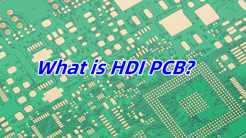
Introduction: The Evolution of PCB Technology
Since the invention of printed circuit boards (PCBs) in the 1930s, electronic innovation has been deeply intertwined with advancements in circuit integration. Traditional PCBs, with through-hole components and single-layer designs, paved the way for modern electronics. However, as devices shrank while demanding higher performance, High-Density Interconnect (HDI) PCBs emerged as a game-changer. By enabling denser component packing, faster signal transmission, and enhanced thermal management, HDI PCBs became indispensable in smartphones, medical devices, aerospace, and AI hardware. This article explores the principles, manufacturing nuances, applications, and future trends of HDI PCB technology, supported by technical data and industry benchmarks.
What is HDI PCB? Defining High-Density Interconnect
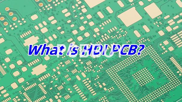
HDI PCBs are advanced printed circuit boards designed to accommodate higher component density and complex electrical connections while maintaining signal integrity and thermal efficiency. Unlike traditional PCBs, HDI PCBs integrate:
-
Microvias: Extremely small vias (typically < 150μm diameter) that enable layer-to-layer routing without large through-holes.
-
Buried and Blind Vias: Internal connections that reduce space waste and improve signal paths.
-
Fine Pitch Routing: Line widths/spacing as low as 3–5μm, allowing compact trace layouts.
-
Multilayer Stacking: Layer counts ranging from 4–60+ layers, depending on application demands.
Key Differentiators from Traditional PCBs
|
Feature |
Traditional PCBs |
HDI PCBs |
|
Typical Via Diameter |
>200μm |
<150μm (down to 30μm) |
|
Line/Space Resolution |
10–20μm |
3–8μm |
|
Max Layer Count |
≤20 layers |
≥40 layers |
|
Common Applications |
Simple consumer electronics |
Smartphones, AI accelerators |
Data Sources: IPC Standards (IPC-2223), Huawei Technical Whitepapers, Samsung Electronics Reports.
The Architecture of HDI PCBs: Layers, Materials, and Design
1. Layer Construction
HDI PCBs consist of core layers (for structural integrity) and buildup layers (for high-density routing). A typical 4+4+4 HDI structure might include:
-
Outer Layers: Component pads and heavy copper for power distribution.
-
Inner Layers: Microvias and buried vias for horizontal/vertical connectivity.
-
Dielectric Substrates: Low-loss materials like PTFE or ceramic-filled epoxy to minimize signal loss.
2. Material Innovations
-
Base Dielectric:
o Traditional: FR-4 (flame-retardant epoxy glass).
o HDI Advancements: High-Tg (glass transition temperature) laminates, IS680 (for high-frequency applications).
Conductive Layers:
o Foil: Copper thickness options (e.g., 0.5oz–10oz) for power/ground planes.
o Plating: ENIG (Electroless NickelImmersion Gold) for corrosion resistance.
3. Microvia Technologies
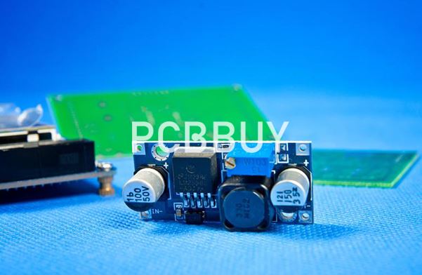
Microvias are the backbone of HDI PCBs. Manufactured via laser drilling or mechanical drilling, their size directly impacts density:
-
Laser Microvias: Precisions down to 25μm, ideal for fine-pitch IC substrates.
-
Stacked Vias: Multiple microvias connected vertically to route dense signals.
Manufacturing Process: Precision at Every Stage
HDI PCB production demands semiconductor-like precision. Key steps include:
1. Image Transfer & Etching
-
Photolithography: Using aligned photomasks to define tiny traces (resolution up to 2μm).
-
Etching: Ferric chloride or plasma etching for precise patterning.
2. Via Formation
-
Laser Ablation: Ytterbium fiber lasers drill 50μm holes at 100k+ speeds.
-
Electroplating: Cu filling with <1% thickness variation across vias.
3. Layer Pressing
-
Massachusetts Lamination: Aligning core and prepreg layers under 35 kg/cm² pressure at 180°C.
-
Resin Filling: Epoxy-based prepreg to fill microvoids and ensure planarity.
4. Surface Finishing
-
ENEPIG: For solderability and anti-oxidation.
-
OSP (Organic Solder Preservative): Benzotriazole coatings for green processing.
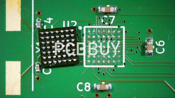
Performance Metrics: Why HDI PCBs Outperform
1. Signal Integrity
-
Impedance Control: Strict tolerances (±10Ω) for high-speed DDR memory buses.
-
Crosstalk Reduction: Spaced traces with 3W design rules (trace width/spacing ratio).
2. Thermal Management
-
Thermal Conductivity: Copper planes dissipate heat at 398 W/m·K, vs. FR-4’s 0.3 W/m·K.
-
Via Heat Paths: Arrayed microvias spread heat in high-power ICs.
3. Reliability Testing
-
Thermal Cycling: Passes -40°C to 125°C cycles (IPC-9701 standards).
-
Mechanical Flexure: Bend tests simulate real-world flexing in portable devices.
Applications Driving HDI Demand
1. Mobile Devices
-
Smartphone motherboards use 8–12 layer HDI PCBs to integrate SoCs, memory, and sensors in <50mm² areas.
-
Example: iPhone logic boards with 4000+ microvias/cm² density.
2. High-Performance Computing
-
AI/ML accelerators demand 20+ layer HDI PCBs for GPU-FPGA interconnects.
-
Data: NVIDIA A100 GPU modules utilize HDI for 10TB/s+ memory bandwidth.
3. Medical Electronics
-
Implantable devices require flexible HDI PCBs with biocompatible laminates (e.g., polyimide).
4. Automotive Radar Systems
-
mmWave radar PCBs with 10GHz+ signal handling use PTFE substrates for low loss.
Challenges and Future Directions
Current Roadblocks
-
Cost: HDI manufacturing costs ~3x–5x that of traditional PCBs due to precision tooling.
-
Yield Rates: Laser drilling defects cause ~5–10% scrap rates in high-layer counts.
-
Environmental Impact: Chemical-intensive processes raise sustainability concerns.
Innovations on the Horizon
-
Panelization Techniques: Multi-board panels reduce per-unit costs by 20%.
-
Additive Manufacturing: 3D printing conductive inks for prototype HDI boards.
-
AI-Driven Design: Machine learning optimization for via placement and layer stacking.
Conclusion: The Future of Electronic Integration
HDI PCB technology is the linchpin of modern electronics, enabling devices to be smaller, faster, and more energy-efficient. As semiconductor nodes shrink and IoT proliferates, HDI PCBs will evolve with:
-
Sub-25μm vias for extreme miniaturization.
-
Embedded passives (resistors/capacitors) to save board space.
-
Sustainable materials like bio-based laminates and recyclable copper foils.
By mastering HDI PCB design and manufacturing, brands can stay at the forefront of innovation, delivering products that meet the dual demands of performance and reliability.
References
-
IPC Standards Handbook (2023 Edition). IPC Association Connecting Electronics Industries.
-
"Advancements in High-Density Interconnect Technology," IEEE Transactions on Components, Packaging, and Manufacturing Technology, Vol. 12, No. 3, 2022.
-
Samsung Electronics, HDI PCB Manufacturing Playbook," 2021 Technical Brief.
-
Huawei Technologies, 5G and Beyond: The Role of HDI PCBs," Whitepaper, 2023.
-
National Physics Laboratory, Thermal Management in High-Density Circuits, Research Report NPL-2020-RR-7.
Industry Category


