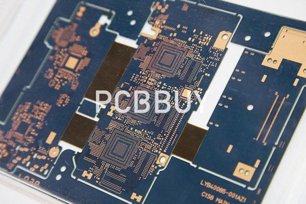
HDI PCB
By:PCBBUY 06/04/2021 17:21

HDI PCB, also known as high-density interconnect PCB, is a kind of PCB with a higher wiring density per unit area than traditional boards. HDI boards are more compact and have smaller vias, pads, copper traces and spaces. As a result, HDIs have denser wiring resulting in lighter weight, more compact, lower layer count PCBs. The lesser weight and size of the HDI circuitry means the PCBs fit into the little spaces and have a smaller amount of mass than conservative PCB designs.
They have more functionality in a small area and a higher circuitry density per unit compared to other PCBs. They can come with a variety of features including but not limited to:
-Through vias and buried vias
-At least two layers with through vias
-Coreless construction with layer pairs
Please check the content below in this passage for more knowledge about HDI PCB.
What are the lamination & material of HDI PCB?
Advanced multilayer technology allows for designers to sequentially add additional pairs of layers to form a multilayer PCB. The use of a laser drill to produce holes in the internal layers allows for plating, imaging and etching prior to pressing. This added process is known as sequential build up. SBU fabrication uses solid filled vias allowing for better thermal management, a stronger inter connect and increasing the board's reliability.
Resin coated copper was developed specifically to aide with poor hole quality, longer drill times and to allow for thinner PCBs. RCC has an ultra-low profile and ultra-thin copper foil that is anchored with minuscule nodules to the surface. This material is chemically treated and primed for the thinnest and finest line and spacing technology.
The application of dry resist to the laminate still uses heated roll method to apply the resist to core material. This older technology process, it is now recommended to preheat the material to a desired temperature prior to the lamination process for HDI printed circuit boards. The preheating of the material allows for better a steady application of the dry resist to the surface of the laminate, pulling less heat away from the hot rolls and allowing for consistent stable exit temperatures of the laminated PCB product. Consistent entrance and exit temperatures lead to less air entrapment beneath the film; this is critical to the reproduction of fine lines and spacing.
What are the advantages of HDI PCB?
The primary benefit of HDI printed circuit boards is the capability to “do more with less”; with copper-etching technology continuously refined for better precision, it became possible to combine functionalities of multiple PCBs into one HDI PCB.

Shortening the distance between devices and trace spaces, HDI PCBs allow for deployment of a large number of transistors for better performance in electronics while lowering power consumption. Signal integrity is also improved due to the shorter distance connections and lower power requirements. Other performance improvements over conventional PCBs include stable voltage rail, minimal stubs, lower RFI/EMI, and closer ground planes and distributed capacitance.
Additionally, consider using a HDI printed circuit board for the following benefits:
Cost-effectiveness: when properly planned out, overall costs are reduced due to the lower number of necessary layers and smaller sizes/fewer number of needed boards when compared to standard PCBs.
Faster time-to-market: Design efficiencies in HDI PCB production mean faster time-to-market. Because of the easy placement of components and vias and electrical performance, it takes a shorter amount of time to go through the design and testing process for HDI PCBs.
Better reliability: Microvias have much better reliability than typical through holes due to the use of a smaller aspect ratio; they are more dependable than through holes, granting HDIs outstanding performance with better materials and parts.
What are uses of HDI PCB?
A HDI PCB is usually found in complex electronic devices that demand excellent performance while conserving space. Applications include mobile /cellular phones, touch-screen devices, laptop computers, digital cameras, 4/5G network communications, and military applications such as avionics and smart munitions.
Automotive and aerospace industries, where lower weight can mean more efficient operation, have been utilizing HDI PCBs at an increasing rate. Like almost everything else, cars are becoming more connected and computerized. Today’s cars have around 50 microprocessors on board that play a role in engine controls, diagnostics, safety features and other conveniences. Many advanced features such as onboard WiFi and GPS, rearview cameras and backup sensors rely on HDI PCBs. As automotive technology continues to advance, HDI tech will likely play an increasingly important role.
HDI PCBs are also prominently featured in medical devices; advanced electronic medical devices such as equipment for monitoring, imaging, surgical procedures, laboratory analysis etc., and incorporate HDI boards. The high-density technology promotes improved performance and smaller, more cost-effective devices, potentially improving the accuracy of monitoring and medical testing.
Industrial automation requires abundant computerization, and IoT devices are becoming more common in manufacturing, warehousing, and other industrial settings. Many of these advanced equipment employ HDI technology. Today, businesses use electronic tools to keep track of inventory and monitor equipment performance. Increasingly, machinery includes smart sensors that collect usage data and connect to the internet to communicate with other smart devices, as well as to relay information to management and help optimize operations.
Industry Category


